Enhancement-Mode III-N Devices, Circuits, and Methods

a technology of enhancement-mode and heterostructure, which is applied in the direction of semiconductor devices, basic electric elements, electrical equipment, etc., can solve the problems of poor performance characteristics of e-mode hfet's fabricated in this manner, large on-resistance, and low transconductance, and achieve high breakdown field, large thermal conductivity, and wide band gap

Active Publication Date: 2007-12-06
THE HONG KONG UNIV OF SCI & TECH
View PDF49 Cites 190 Cited by
  • Summary
  • Abstract
  • Description
  • Claims
  • Application Information

AI Technical Summary

Benefits of technology

[0002] The present application relates to structures and methods of fabricating enhancement-mode heterostructure field effect transistors (“HFETs”), and in particular, to aluminum-gallium-nitride / gallium-nitride (“AlGaN / GaN”) enhancement-mode HFETs. Group III-nitride (“III-N”) compound semiconductors, such as those incorporating AlGaN / GaN, possess the advantages of having wide bandgap, high breakdown field, and large thermal conductivity, which can bring significant benefits to the design of heterostructure field-effect transistors and applications ultilizing HFETs. Because their high power handling capabilities, AlGaN / GaN HFETs can be used for radio frequency / microwave power amplifiers and high power switches. However, most power amplifiers and switches using AlGaN / GaN HFETs feature depletion-mode (“D-mode”) HFETs as the building block. Since a D-mode HFET is a transistor with a negative value for the threshold voltage (“Vth”), D-mode HFETs need both a positive and negative voltage bias to be turned on and off. If an enhancement-mode (“E-mode”) HFET could be made available, only a positive voltage supply would be needed for circuit applications, resulting in simplified circuits and reduced costs.
[0008] Another attempt to fabricate an E-mode HFET in an AlGaN / GaN system was reported by Hu et al., “Enhancement mode AlGaN / GaN HFET with selectively grown PN junction gate,” April 2000, IEE Electronics Letters, Vol. 36, No. 8, pp. 753-754, which is hereby incorporated by reference in its entirety. In this work a selectively-grown P / N junction gate is used. The selectively-grown P-type layer is able to raise the potential of the channel and therefore deplete the carriers from the channel at zero gate bias. However, such an approach is not self-aligned and the problem of large access resistance persists.
[0014] The present application describes a new family of approaches to III-N device fabrication. According to various embodiments, fluorine ions are introduced into the wider-bandgap layer under the gate electrode as a step in the fabrication of a HEMT or the like. The implanted ions are substantially immobile and can effectively deplete the electrons in the channel underneath. Rapid thermal annealing as a further fabrication step fully repairs degradation of the carrier mobility in the channel without any other adverse effects to the HFETs. The resulting HFET has an access region between the source and gate electrodes that possesses high carrier density in the channel while maintaining low access resistance.
[0015] The disclosed innovations, in various embodiments, provide on or more of at least the following advantages:

Problems solved by technology

However, E-mode HFET's fabricated in this manner have poor performance characteristics, such as low transconductance, large on-resistance, and high knee-voltage.
Note that gates that are not self-aligned require overlap, which increases device size and stray capacitance.
However, such an approach is not self-aligned and the problem of large access resistance persists.
However, ICP-RIE can cause serious damage to the AlGaN barrier and results in increased gate leakage current.
Thus, the gate patterns have to be created again through photo-lithography which cannot be accurately aligned with the recess-etching windows previously generated in the gate recess stage.
Another problem associated with the ICP-RIE etching is the poor uniformity in the etching depth, which is undesirable for integrated circuits because it severely affects the uniformity in the threshold voltage.
However, in an AlGaN / GaN HFET, because of the lack of effective wet etching techniques, the recess etching is carried out by dry etching.
For example, ICP-RIE is used for the recess etching, as mentioned earlier, with the accompanying severe damage and defects to the device.
However, no metal has been found to have a work function larger than 1 electron volt (“eV”).
This is not suitable for the integration of E-mode and D-mode HEMTs, which are both required for DCFL circuits.

Method used


Image

  • Enhancement-Mode III-N Devices, Circuits, and Methods
  • Enhancement-Mode III-N Devices, Circuits, and Methods
  • Enhancement-Mode III-N Devices, Circuits, and Methods

Examples


example 1

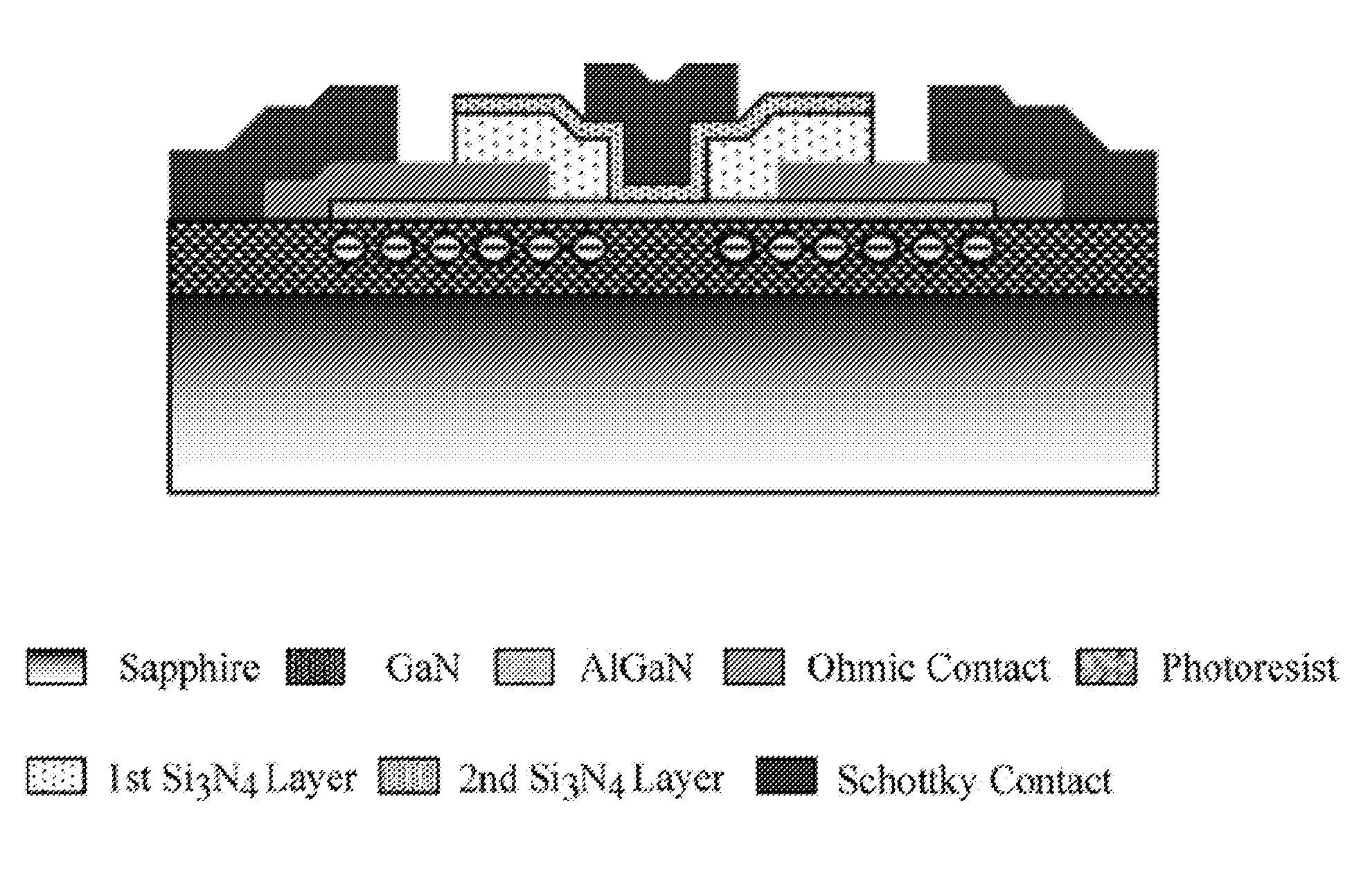
[0059] An AlGaN / GaN HEMT structure was grown on a (0001) sapphire substrate in an Aixtron AIX 2000 HT metal-organic chemical vapor deposition (MOCVD) system. The HEMT structure consists of a low-temperature GaN nucleation layer, a 2.5-m-thick unintentionally doped GaN buffer layer and an AlGaN barrier layer with nominal 30% Al composition. The barrier layer consists of a 3-nm undoped spacer, a 15-nm carrier supplier layer doped at 2.5×1018 cm−3, and a 2-nm undoped cap layer. Room temperature Hall measurements of the structure yield an electron sheet density of 1.3×1013 cm−2 and an electron mobility of 1000 cm2 / Vs. The device mesa was formed using Cl2 / He plasma dry etching in an STS ICP-RIE system followed by the source / drain ohmic contact formation with Ti / Al / Ni / Au annealed ate 850° C. for 45 seconds. The ohmic contact resistance was typically measured to be 0.8 ohn-nm.

[0060] After gate windows with 1 nm length were opened by contact photolithography, the sample was treated by CF4 ...


PUM


Abstract

A method of fabricating AlGaN / GaN enhancement-mode heterostructure field-effect transistors (HFET) using fluorine-based plasma immersion or ion implantation. The method includes: 1) generating gate patterns; 2) exposing the AlGaN / GaN heterostructure in the gate region to fluorine-based plasma treatment with photoresist as the treatment mask in a self-aligned manner; 3) depositing the gate metal to the plasma treated AlGaN / GaN heterostructure surface; 4) lifting off the metal except the gate electrode; and 5) high temperature post-gate annealing of the sample. This method can be used to shift the threshold voltage of a HFET toward a more positive value, and ultimately convert a depletion-mode HFET to an enhancement-mode HFET (E-HFET).

Description

CROSS-REFERENCE TO RELATED APPLICATIONS [0001] This application claims priority from U.S. Provisional Patent Application No. 60 / 740,256 filed on Nov. 29, 2005, and also from U.S. Provisional Patent Application No. 60 / 748,339 filed on Dec. 8, 2005, both of which are hereby incorporated by reference.BACKGROUND AND SUMMARY OF THE INVENTION [0002] The present application relates to structures and methods of fabricating enhancement-mode heterostructure field effect transistors (“HFETs”), and in particular, to aluminum-gallium-nitride / gallium-nitride (“AlGaN / GaN”) enhancement-mode HFETs. Group III-nitride (“III-N”) compound semiconductors, such as those incorporating AlGaN / GaN, possess the advantages of having wide bandgap, high breakdown field, and large thermal conductivity, which can bring significant benefits to the design of heterostructure field-effect transistors and applications ultilizing HFETs. Because their high power handling capabilities, AlGaN / GaN HFETs can be used for radio...

Claims


Application Information

Patent Timeline
Patent Type & Authority Applications(United States)
IPC IPC(8): H01L31/00
CPCH01L29/2003H01L29/7787H01L29/66462
Inventor CHEN, JINGCAI, YONGLAU, KEI MAY
Owner THE HONG KONG UNIV OF SCI & TECH
Why Eureka
Try Eureka