

Method for enhancing ohmic contact of gallium oxide semiconductor device
A technology of ohmic contact and gallium oxide, which is applied in the direction of semiconductor devices, electrical components, circuits, etc., can solve the problems of large power loss of gallium oxide power devices, the inability to realize industrialization, and large ohmic contact resistance, etc. The effect of low and high breakdown field strength
- Summary
- Abstract
- Description
- Claims
- Application Information
AI Technical Summary
Problems solved by technology
Method used
Image

Examples
Embodiment Construction
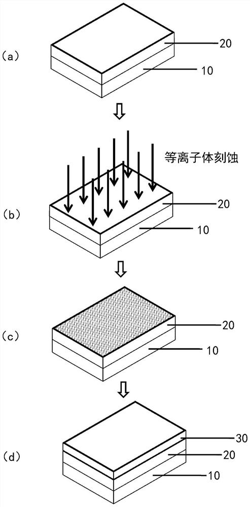
[0027] The present disclosure provides a method for enhancing the ohmic contact of a gallium oxide semiconductor device. The plasma etching technology is used to treat the surface of the gallium oxide semiconductor device, and the roughness, oxygen dangling bonds, Oxygen vacancies and other parameters make the subsequent metal deposited on the gallium oxide semiconductor form a very thin tunnel oxide layer, reduce the Schottky barrier, weaken the influence of the Schottky contact, enhance the ohmic contact, and reduce the Contact resistance. This method is helpful to promote the use of gallium oxide materials. In addition, the use of plasma etching to improve ohmic contacts is not limited to gallium oxide materials, and can also be extended to other semiconductor devices.
[0028] In order to make the purpose, technical solutions and advantages of the present disclosure clearer, the present disclosure will be further described in detail below in conjunction with specific embod...
PUM
 Abstract
Description
Claims
Application Information