Photovoltaic device

Inactive Publication Date: 2012-01-12
MITSUBISHI HEAVY IND LTD
View PDF4 Cites 3 Cited by
  • Summary
  • Abstract
  • Description
  • Claims
  • Application Information

AI Technical Summary

Benefits of technology

[0016]The photovoltaic device of the present invention provides a titanium oxide film as an intermediate contact layer, and therefore increases the amount of incident light entering the backside electric power generation layer. Further, by also providing a backside transparent conductive film as an intermediate contact layer, favorable electrical contact properties and good

Problems solved by technology

However, with a single-layer intermediate contact layer, a problem arises in that the amount of incident light entering the crystalline silicon layers is dramatically reduced.
Even if the refractiv

Method used


Image

  • Photovoltaic device
  • Photovoltaic device
  • Photovoltaic device

Examples


example 1

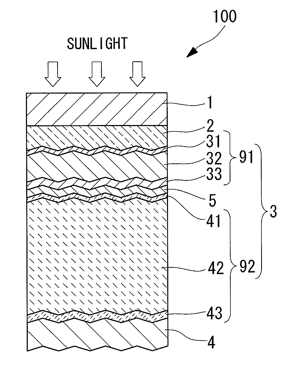
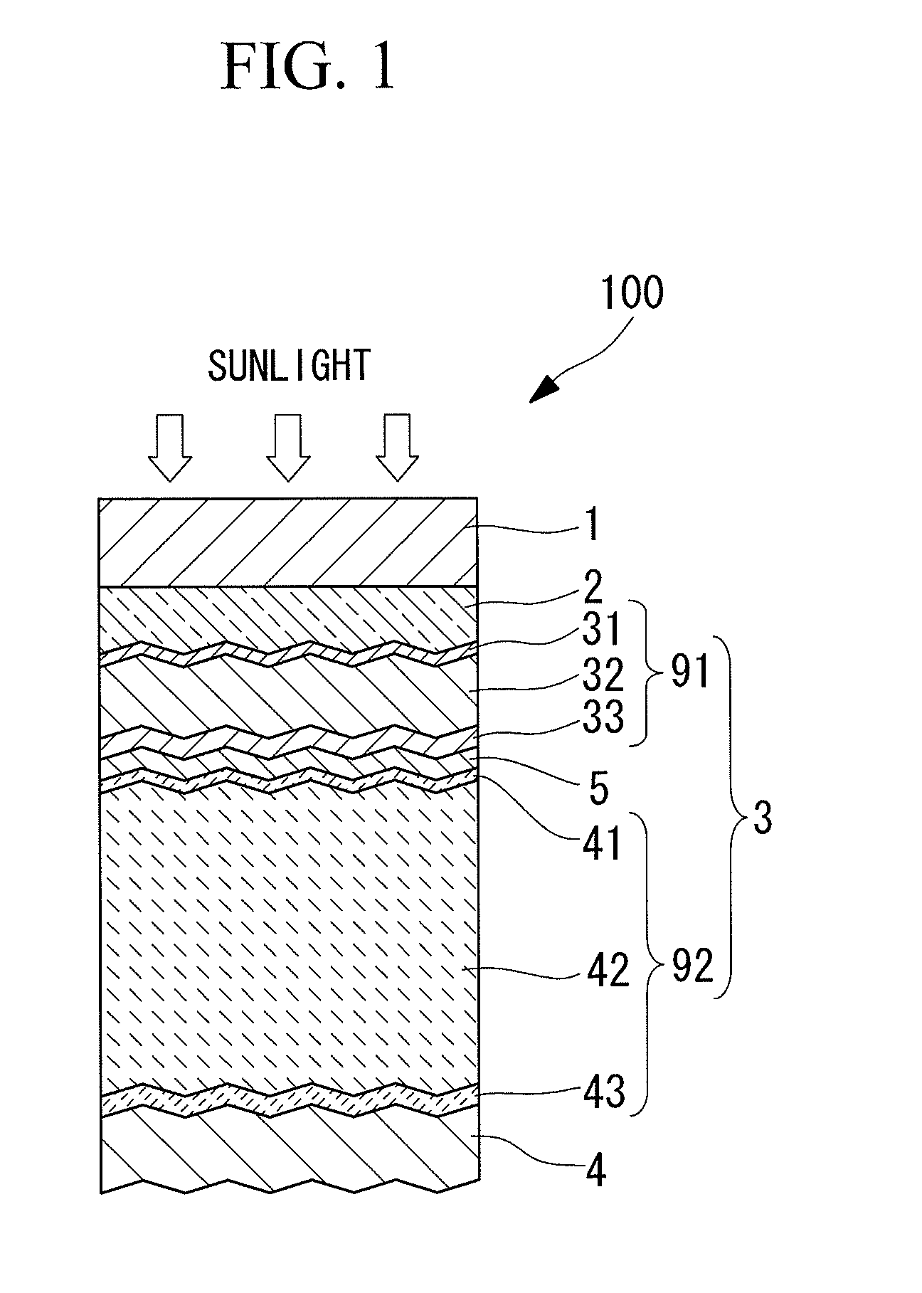
[0055]An optical analysis calculation for a tandem solar cell of the structural model illustrated in FIG. 6 was performed using a FDTD (Finite Difference Time Domain) method for the case where incident light enters the solar cell from the side of the glass substrate 1, and a light absorption spectrum was determined for each layer. The value calculated by integrating the product obtained by multiplying the absorption spectrum and the sunlight spectrum (AM 1.5) was used as the electric current. The size of one pixel of the structural model was 10 nm. The structural model was a pseudo two-dimensional model, and optical analysis calculations were performed for light of two polarization directions (p-polarized light and s-polarized light), with the average value of the two results being used as the solution. p-polarized light refers to light in which the electric field vector is parallel to the surface of the page in FIG. 6, whereas s-polarized light refers to light in which the electric...

example 2

[0085]The structure and thickness of each of the layers in Example 2 were the same as those in Example 1.

[0086]In Example 2, the haze ratio of the transparent electrode layer (the substrate having the transparent electrode layer provided thereon) in the structural model illustrated in FIG. 6 was 30%, the pitch of the textured structure of the transparent electrode layer 2 was 1 μm, and the inclination angle was 30°. A structural model was used in which the surface shapes of the first cell i-layer 32 and the second cell i-layer 42 were determined from the results of AFM shape analysis.

[0087]In Example 2, optical analysis calculations were used to prepare a short-circuit current distribution diagram similar to that of Example 1. In Example 2, the thickness region that yielded an increase in the short-circuit current tended to shift slightly towards a thinner titanium oxide film compared with the thickness region that yielded an increase in the short-circuit current in Example 1.

[0088]...


PUM


Abstract

A photovoltaic device comprising an intermediate contact layer for which the reflection characteristics have been optimized. The photovoltaic device (100) comprises a transparent electrode layer (2), which is disposed on a substrate (1) and has a textured structure on the surface opposite the substrate (1), a photovoltaic layer (3) composed of two electric power generation layers (91, 92), a back electrode layer (4), and an intermediate contact layer (5) disposed between the two electric power generation layers (91, 92), wherein the intermediate contact layer (5) comprises a titanium oxide film comprising mainly titanium oxide and a backside transparent conductive film comprising mainly a transparent conductive oxide, with the titanium oxide film disposed nearer the substrate (1), and the thickness of the titanium oxide film is a value that falls within a range defined as being from 65 to 110 nm inclusive when the thickness of the backside transparent conductive film is 5 nm, and similarly, from 65 to 95 nm inclusive when 10 nm, from 65 to 90 nm inclusive when 15 nm, from 60 to 85 nm inclusive when 20 nm, from 55 to 70 nm inclusive when 25 nm, and from 55 to 65 nm inclusive when 30 nm.

Description


Claims


Application Information

Patent Timeline
Owner MITSUBISHI HEAVY IND LTD
Why Eureka
Try Eureka