
Amplifier with wide gain range

a wide gain and amplifier technology, applied in the direction of low-noise amplifiers, gated amplifiers, amplifier combinations, etc., can solve the problems of increased noise level at low gain, noise getting worse, extra signal loss, etc., and achieve the effect of wide gain range and reduced noise level

Active Publication Date: 2012-01-12
NOVATEK MICROELECTRONICS CORP
View PDF1 Cites 2 Cited by
  • Summary
  • Abstract
  • Description
  • Claims
  • Application Information

AI Technical Summary

Benefits of technology

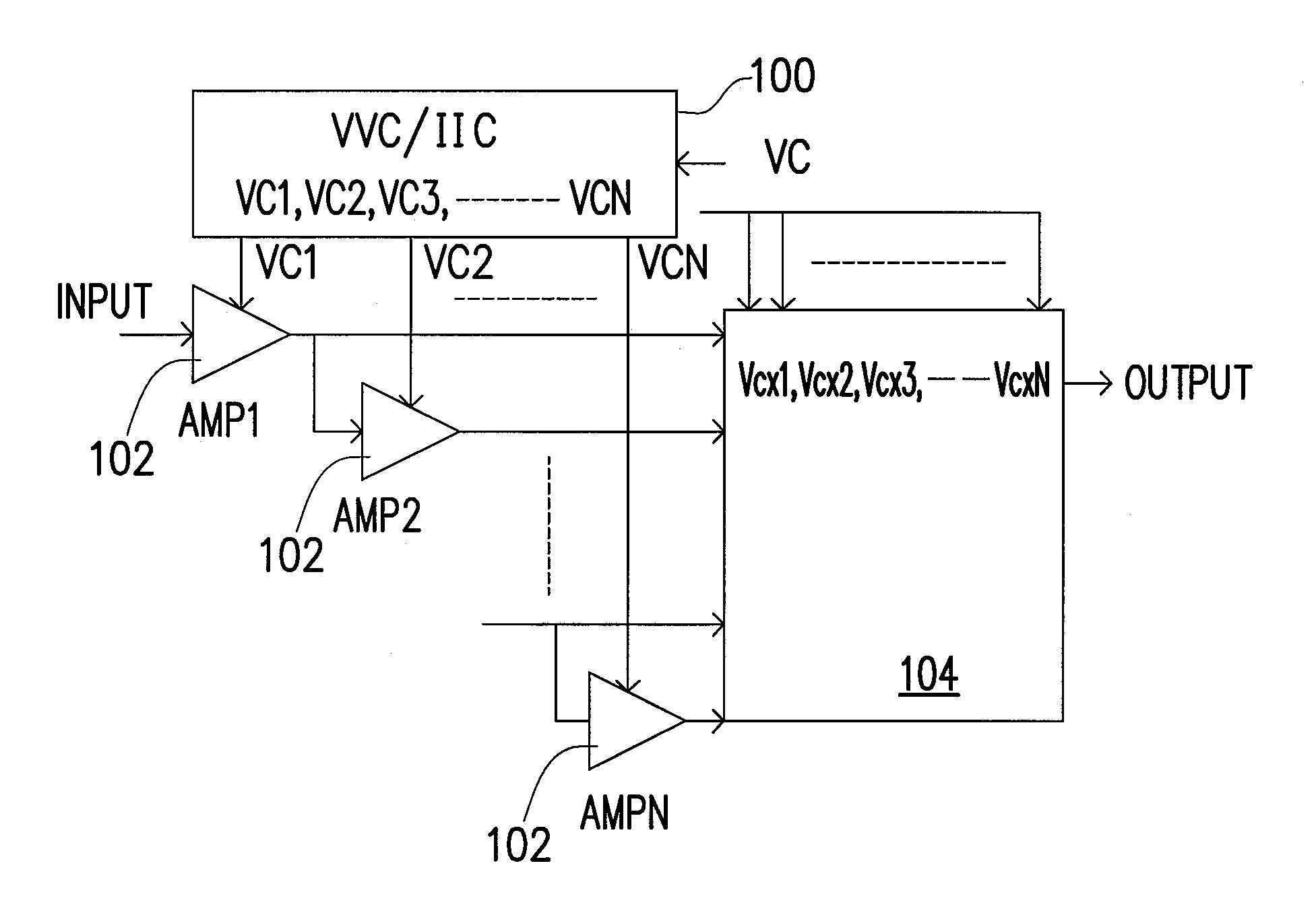
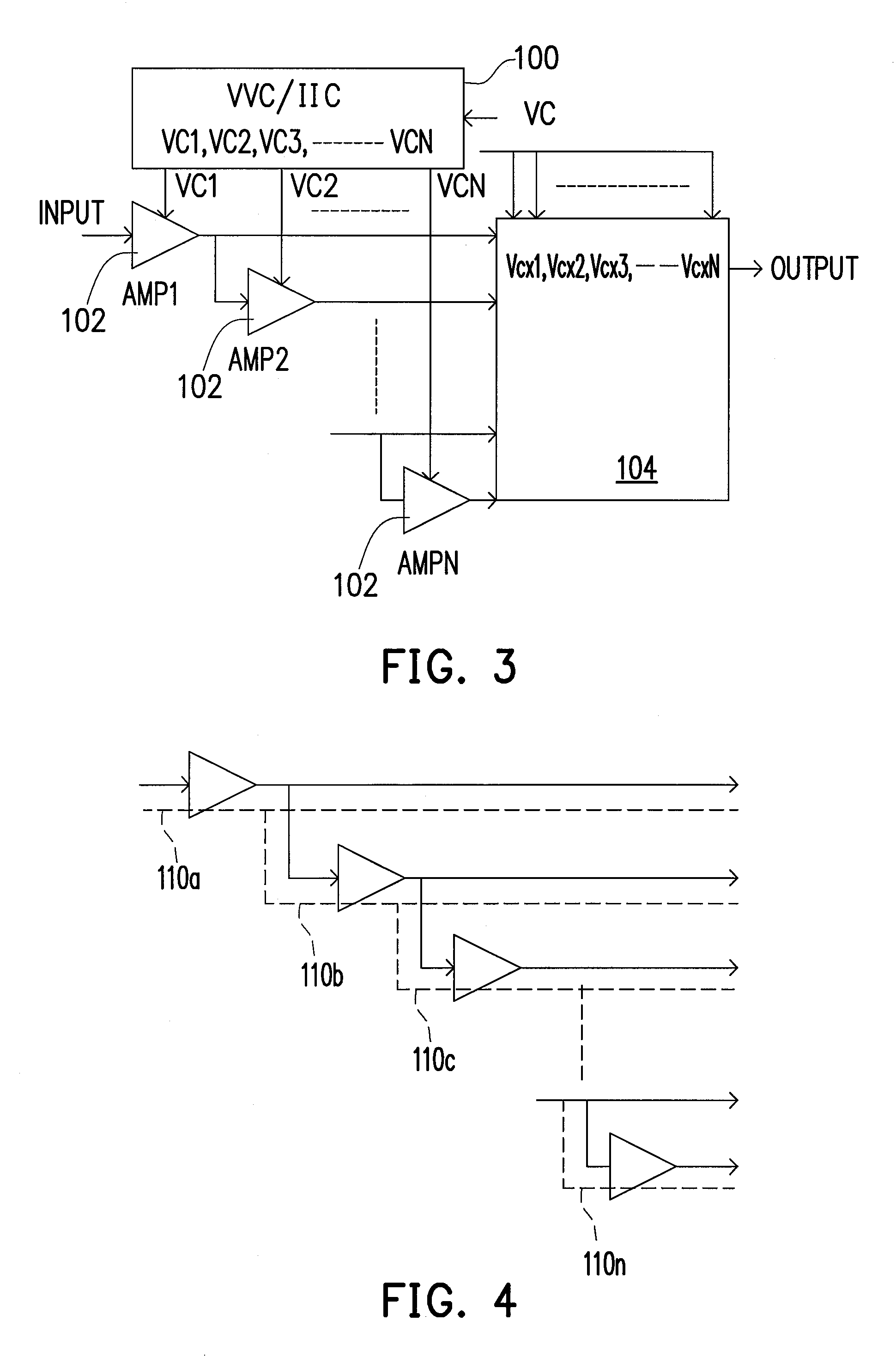
The invention provides an amplifier with a wide gain range and reduced noise levels. The amplifier has a signal converting unit that receives a gain modulation signal and outputs multiple modulation signals and selection signals. The channel unit has multiple channels, each controlled by a selection signal, so as to conduct the channel with the selected state. The amplifiers are connected in series and output their output terminals to the channels of the channel unit. The amplifiers are also controlled by the modulation signals of the signal converting unit. The gain modulation method involves outputting multiple modulation signals and selection signals, implementing multiple channels, and controlling each amplifier with a modulation signal. The technical effects of the invention include a wider range of gain and reduced noise levels.

Problems solved by technology

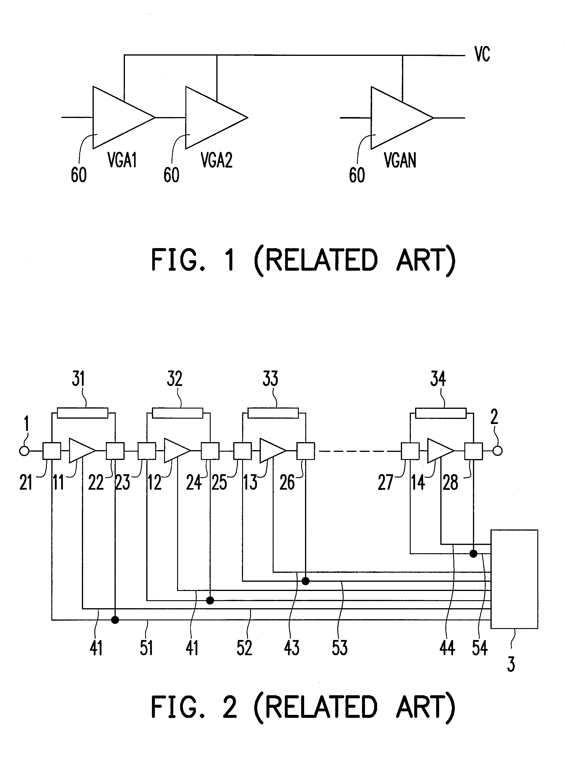
For the circuit structure in FIG. 1, when it is operated at a low gain, each amplifier 600 is turned on, resulting in high noise level at the low gain.
As a result, the extra loss of signal occurs, and the noise gets worse.
In other words, although the variable gain range can be formed by connecting multiple amplifiers, it causes larger noise level when it is operated at low gain level because multiple amplifiers are connected together.

Method used


Image

  • Amplifier with wide gain range
  • Amplifier with wide gain range
  • Amplifier with wide gain range

Examples


Embodiment Construction

[0024]The amplifier with wide gain range can have various applications in electronic products. As an example to a receiver, the amplifier with wide gain range at low noise level is the essential part. For the conventional variable gain amplifier, in order to have larger gain range, it usually has a relative low noise level when a gain is operated about the maximum. However, as the need of the system specification, the noise level is still required to be low when the gain is operated at the other gain range. The invention can at least have relatively low noise level for the wide gain range.

[0025]Several embodiments are provided for describing the invention. However, the invention is not just limited to the embodiments. In addition, the embodiments can also be properly combined.

[0026]FIG. 3 is a drawing, schematically illustrating a circuit block structure of amplifier with wide gain range, according to an embodiment of the invention. In FIG. 3, the amplifier with wide gain rage inclu...


PUM


Abstract

An amplifier with wide gain range includes a signal converting unit, a channel unit, and multiple amplifiers. The signal converting unit receives a gain modulation signal and accordingly outputs multiple modulation signals and multiple selection signals. Based on a level of the gain modulation signal, one of the selection signals is set at a first logic state and the other selection signals are at a second logic state. The channel unit has multiple channels, respectively controlled by the selection signals, so as to conduct the channel with at the first logic state. The amplifiers are connected in series. Output terminals of the amplifiers are also respectively output to the channels of the channel unit. The amplifiers are also controlled by the modulation signals of the signal converting unit.

Description

CROSS-REFERENCE TO RELATED APPLICATION[0001]This application claims the priority benefit of Taiwan application serial no. 99122176, filed on Jul. 6, 2010. The entirety of the above-mentioned patent application is hereby incorporated by reference herein and made a part of specification.BACKGROUND OF THE INVENTION[0002]1. Field of Invention[0003]The present invention relates to amplifier with wide gain range, and more particularly to amplifier with wide gain range, which has low noise level.[0004]2. Description of Related Art[0005]Generally, for a single signal amplifier, its gain value is within a limited range. If it needs more gain value to have higher amplification of signal, usually, several amplifiers are connected in series. FIG. 1 is a drawing, schematically illustrating a conventional circuit of variable gain amplifier. In FIG. 1, the conventional variable gain amplifier is formed by several amplifiers 60, coupled in series. The amplifiers 60 respectively have gain ranges of ...

Claims


Application Information

Patent Timeline
Patent Type & Authority Applications(United States)
IPC IPC(8): H03F1/00
CPCH03F1/0277H03F1/26H03F3/189H03F3/72H03F2200/249H03G1/0088H03F2200/405H03F2200/417H03F2200/78H03F2203/7236H03F2200/294
Inventor CHIU, YING-CHUNG
Owner NOVATEK MICROELECTRONICS CORP
Learn More