Plasma etching apparatus and plasma etching method

a technology of plasma etching and plasma, which is applied in the direction of electrical equipment, decorative arts, electric discharge tubes, etc., can solve the problem that the uniform etching shape cannot be formed on the processing target substrate by the etching, and achieve the effect of uniform surface of the processing target substrate and improved cd bias control

Active Publication Date: 2012-01-19
TOKYO ELECTRON LTD
View PDF11 Cites 215 Cited by
  • Summary
  • Abstract
  • Description
  • Claims
  • Application Information

AI Technical Summary

Benefits of technology

[0029]In accordance with the above-described plasma processing apparatus and plasma processing method, the reactant gas can be uniformly supplied to the entire processing target substrate by the first reactant gas supply unit for supplying the reactant gas toward the central region of the processing target substrate and the second reactant gas supply unit for supplying the reactant gas in a directly downward direction toward the focus ring. Further, a stay region where bot

Problems solved by technology

If the CD bias at the central portion and the CD bias at the edge portion are different from each other, uniform etching shapes cannot be formed on the processing target substrate by the etching.
In su

Method used


Image

  • Plasma etching apparatus and plasma etching method
  • Plasma etching apparatus and plasma etching method
  • Plasma etching apparatus and plasma etching method

Examples


Embodiment Construction

[0044]Hereinafter, embodiments of the present invention will be described with reference to the accompanying drawings.

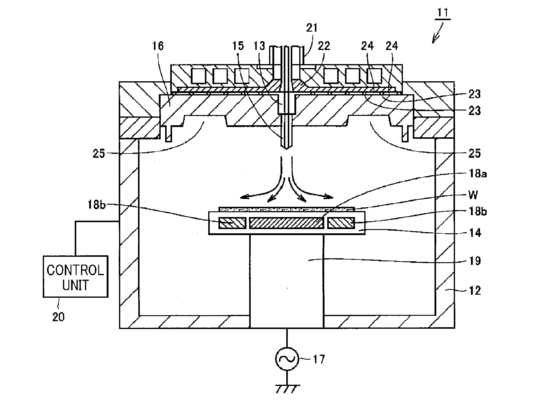
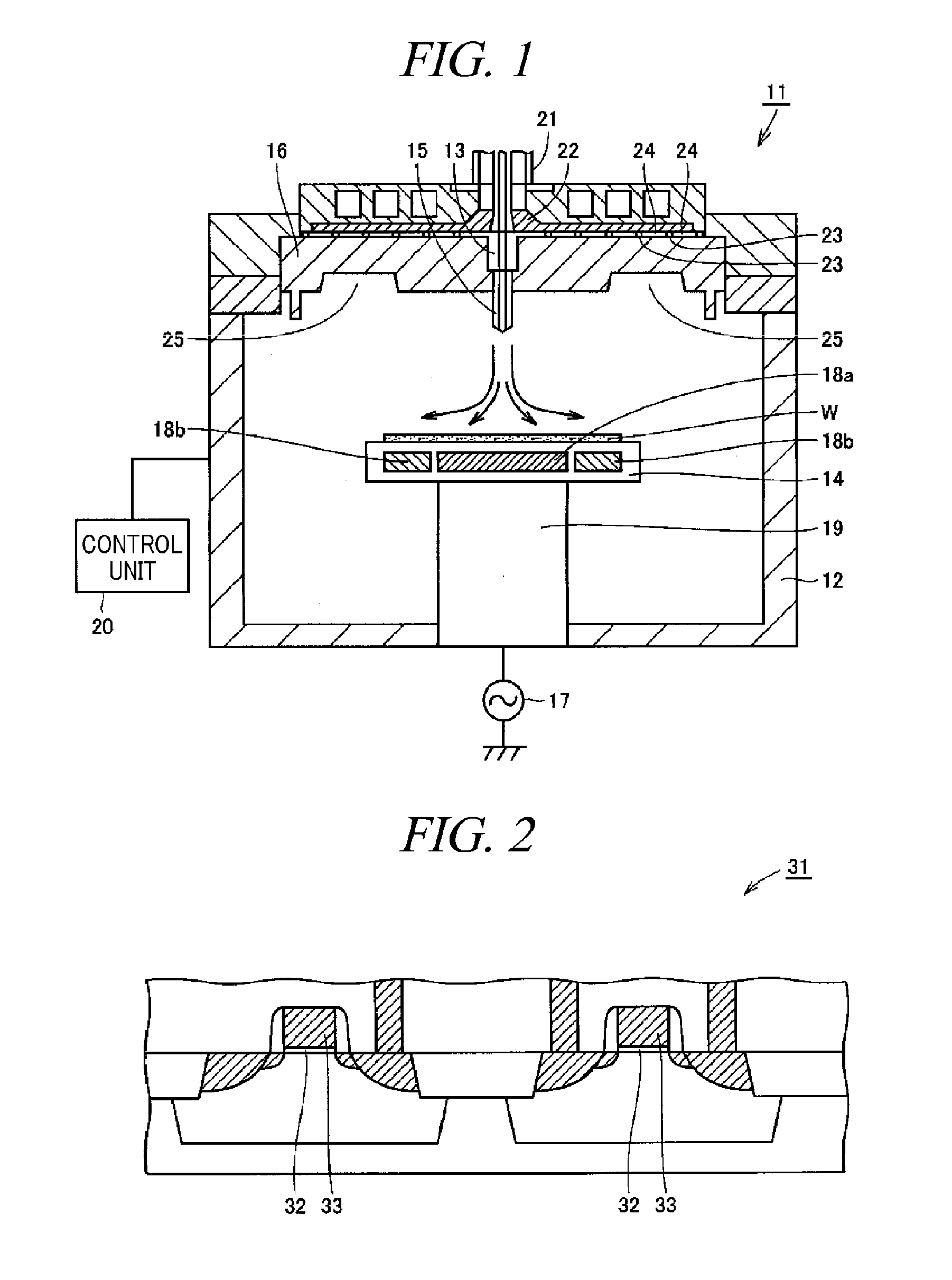
[0045]FIG. 1 is a schematic cross sectional view illustrating major parts of a plasma etching apparatus in accordance with an embodiment of the present invention. In the drawings, the upside of the paper surface is regarded as an upward direction.

[0046]Referring to FIG. 1, a plasma etching apparatus 11 is of a center gas introduction type. The plasma etching apparatus 11 includes a processing chamber 12 configured to perform therein a plasma process on a semiconductor substrate W as a processing target substrate; a reactant gas supply unit 13 having an injector 15 serving as a reactant gas supply port and configured to supply a reactant gas for plasma etching toward a central portion of the semiconductor substrate W; a circular plate-shaped mounting table 14 provided within the processing chamber 12 and configured to hold the semiconductor substrate W thereon; a micr...


PUM

PropertyMeasurementUnit
Temperatureaaaaaaaaaa
Diameteraaaaaaaaaa
Shapeaaaaaaaaaa

Abstract

A plasma etching apparatus 11 includes a mounting table that holds a semiconductor substrate W thereon; a first heater 18a that heats a central region of the semiconductor substrate W held on the mounting table 14; a second heater 18b that heats an edge region around the central region of the semiconductor substrate W held on the mounting table 14; a reactant gas supply unit 13 that supplies a reactant gas for a plasma process toward the central region of the semiconductor substrate W held on the mounting table 14; and a control unit 20 that performs a plasma etching process on the semiconductor substrate W while controlling the first heater 18a and the second heater 18b to heat the central region and the edge region of the processing target substrate W held on the mounting table 14 to different temperatures.

Description

TECHNICAL FIELD [0001]The present invention relates to a plasma etching apparatus and a plasma etching method; and, more particularly, to a plasma etching apparatus and a plasma etching method for generating plasma by using a microwave as a plasma source.BACKGROUND ART [0002]A semiconductor device such as a LSI (Large Scale Integrated circuit) is manufactured by performing a multiple number of processes such as etching, CVD (Chemical Vapor Deposition) and sputtering on a semiconductor substrate (wafer) as a processing target object. As for the processes such as the etching, the CVD and the sputtering, there are plasma etching, plasma CVD, plasma sputtering, and the like using plasma as an energy supply source.[0003]A plasma processing apparatus using a microwave as a plasma generation source is disclosed in Japanese Patent Laid-open Publication No. 2005-100931. In the plasma processing apparatus disclosed in Japanese Patent Laid-open Publication No. 2005-100931, a tapered protrusion...

Claims


Application Information

Patent Timeline
IPC IPC(8): C23F1/00C23F1/08
CPCH01J37/32192H01J37/32935H01L21/67248H01L21/32137H01L21/67109H01J2237/2001
Inventor MATSUMOTO, NAOKITAKAI, KAZUTOKO, REIKAOKAYAMA, NOBUYUKI
Owner TOKYO ELECTRON LTD
Why Eureka
Try Eureka