Memory arrays having substantially vertical, adjacent semiconductor structures and the formation thereof

a technology of memory arrays and semiconductor structures, applied in the field of memory, can solve the problems of severe short channel effect and cell operation problems

Active Publication Date: 2012-01-19
MICRON TECH INC
View PDF6 Cites 85 Cited by
  • Summary
  • Abstract
  • Description
  • Claims
  • Application Information

AI Technical Summary

Problems solved by technology

Smaller dimensions of some device elements may cause operational problems with the cell.
For example, the

Method used


Image

  • Memory arrays having substantially vertical, adjacent semiconductor structures and the formation thereof
  • Memory arrays having substantially vertical, adjacent semiconductor structures and the formation thereof
  • Memory arrays having substantially vertical, adjacent semiconductor structures and the formation thereof

Examples


Embodiment Construction

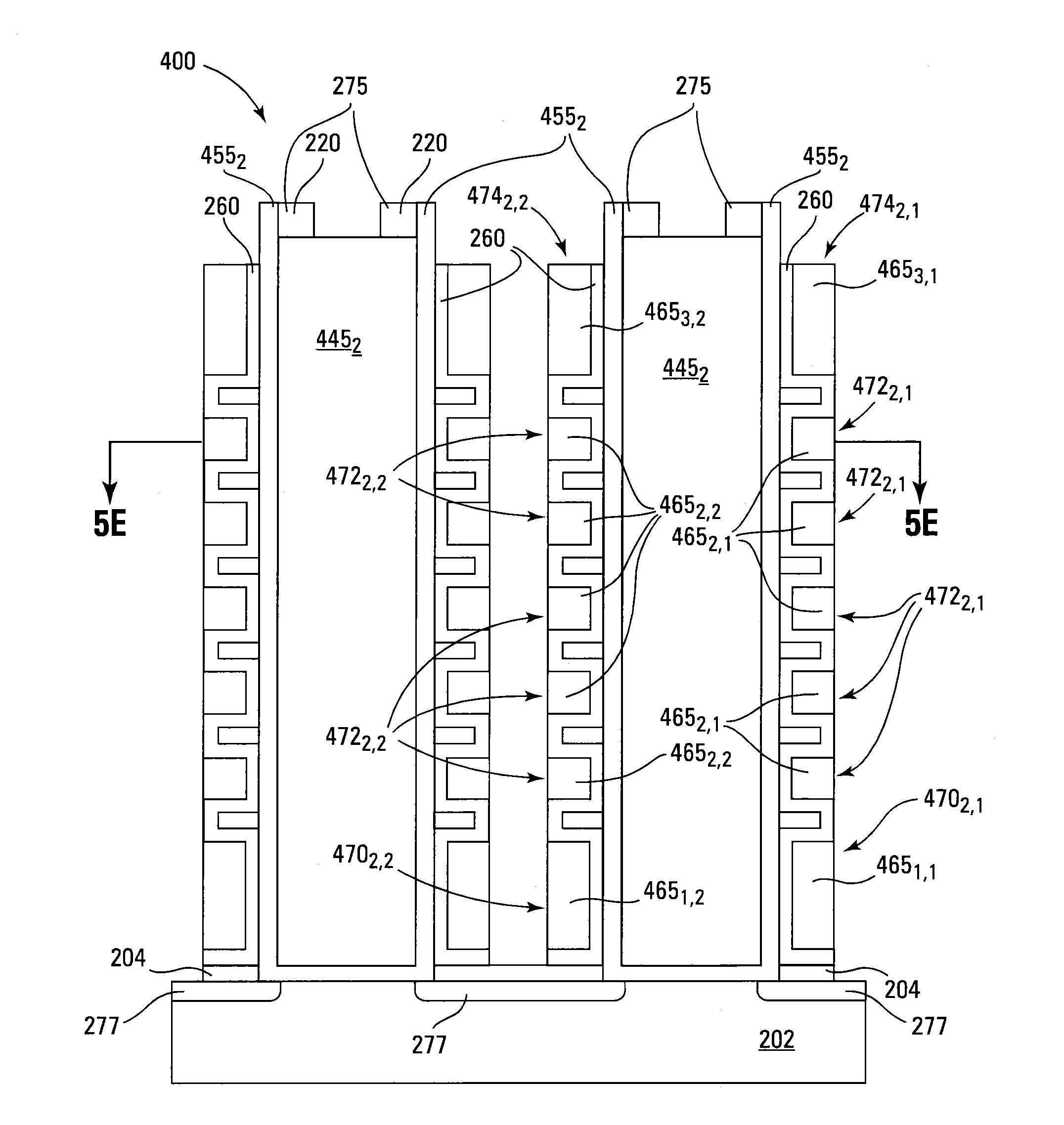
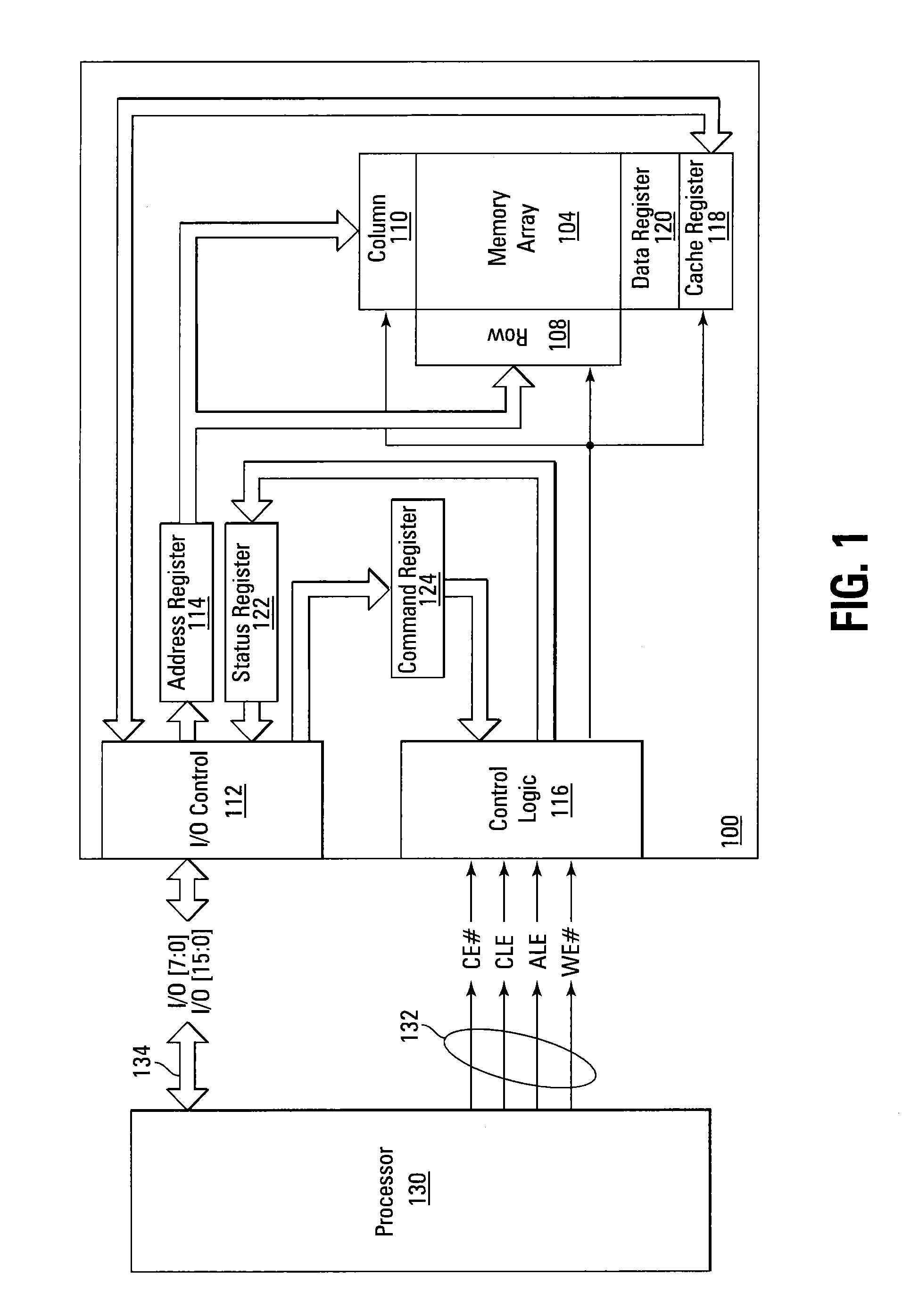
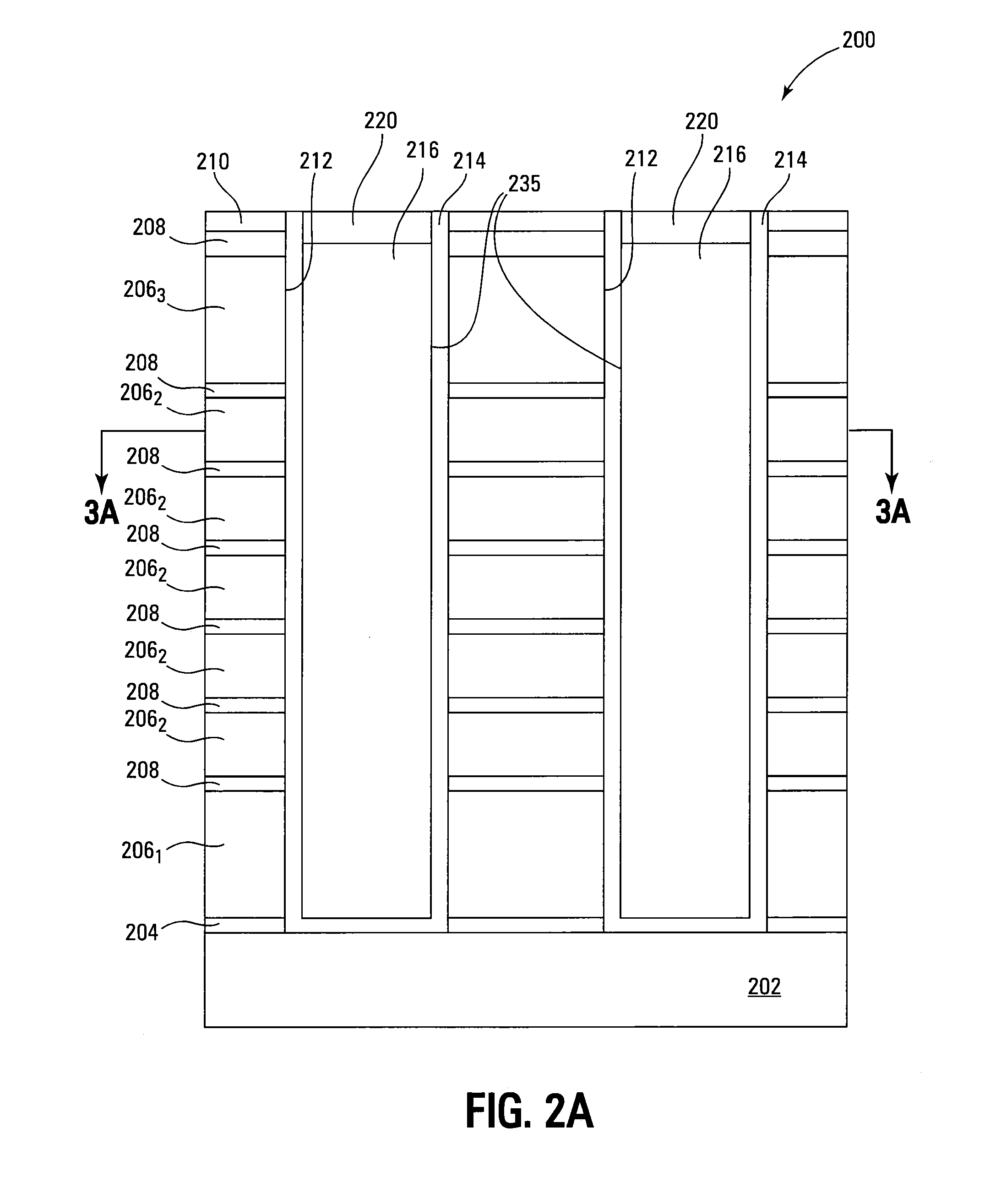
[0015]In the following detailed description, reference is made to the accompanying drawings that form a part hereof, and in which is shown, by way of illustration, specific embodiments. In the drawings, like numerals describe substantially similar components throughout the several views. Other embodiments may be utilized and structural, logical, and electrical changes may be made without departing from the scope of the present disclosure. The following detailed description is, therefore, not to be taken in a limiting sense, and the scope of the present disclosure is defined only by the appended claims and equivalents thereof. The term semiconductor can refer to, for example, a layer of material, a wafer, or a substrate, and includes any base semiconductor structure. “Semiconductor” is to be understood as including silicon-on-sapphire (SOS) technology, silicon-on-insulator (SOI) technology, thin film transistor (TFT) technology, doped and undoped semiconductors, epitaxial layers of a...


PUM


Abstract

Memory arrays and methods of their formation are disclosed. One such memory array has memory-cell strings are formed adjacent to separated substantially vertical, adjacent semiconductor structures, where the separated semiconductor structures couple the memory cells of the respective strings in series. For some embodiments, two dielectric pillars may be formed from a dielectric formed in a single opening, where each of the dielectric pillars has a pair of memory-cell strings adjacent thereto and where at least one memory cell of one of the strings on one of the pillars and at least one memory cell of one of the strings on the other pillar are commonly coupled to an access line.

Description

FIELD[0001]The present disclosure relates generally to memories, and, in particular, in some embodiments, the present disclosure relates to memory arrays having substantially vertical, adjacent semiconductor structures and the formation thereof.BACKGROUND[0002]Memory devices are typically provided as internal, semiconductor, integrated circuits in computers or other electronic devices. There are many different types of memory including random-access memory (RAM), read only memory (ROM), dynamic random access memory (DRAM), synchronous dynamic random access memory (SDRAM), and flash memory.[0003]Flash memory devices have developed into a popular source of non-volatile memory for a wide range of electronic applications. Non-volatile memory is memory that can retain its data values for some extended period without the application of power. Flash memory devices typically use a one-transistor memory cell that allows for high memory densities, high reliability, and low power consumption. ...

Claims


Application Information

Patent Timeline
IPC IPC(8): H01L27/088H01L21/8239
CPCH01L27/11565H01L27/11582H01L27/1157H01L29/7926H01L27/088H10B43/10H10B43/35H10B43/27H10B63/80
Inventor LIU, ZENGTAO
Owner MICRON TECH INC
Why Eureka
Try Eureka