Semiconductor device and method for forming the same

a semiconductor device and semiconductor technology, applied in the field of semiconductor devices, can solve the problems of increasing the difficulty of forming a minute content hole, tungsten (w) and aluminum (al), and affecting the integration of the semiconductor device, so as to prevent the increase of contact resistance and improve the integration effect of the semiconductor devi

Active Publication Date: 2012-01-19
SK HYNIX INC
View PDF5 Cites 3 Cited by
  • Summary
  • Abstract
  • Description
  • Claims
  • Application Information

AI Technical Summary

Benefits of technology

[0011]An object of the present invention is to provide a semiconductor device which prevents contact resistance from being increased when a contact plug is formed, such that it can solve the conventional problems resulting when a contact hole is reduced in width in proportion to higher integration of the semiconductor device.

Problems solved by technology

Generally, although tungsten (W) and aluminum (Al) are basically used to form a metal line and a metal contact plug, the tungsten (W) and the aluminum (Al) may encounter problems caused by electro-migration or stress-migration.
As the semiconductor device is highly integrated, the difficulty in forming a minute content hole is also increasing.
As a result, a defect due to high resistance may occur in the semiconductor device, which makes it difficult for the dual damascene process to be applied for a low-power semiconductor device.
Further, when the dual damascene process is applied to the manufacturing process of the semiconductor device with a narrowly scaled down contact hole, it is probable that the contact hole is not fully filled up by conductive material and thus creates a void in the contact plug.
If copper (Cu) fills up the contact hole, copper atoms may diffuse into an neighboring device element to cause contamination.
However, due to miniaturization, the barrier metal layer cannot be formed thick enough to prevent copper migration.

Method used


Image

  • Semiconductor device and method for forming the same
  • Semiconductor device and method for forming the same
  • Semiconductor device and method for forming the same

Examples


Embodiment Construction

[0035]Reference will now be made in detail to embodiments of the present invention, examples of which are illustrated in the accompanying drawings. Wherever possible, the same reference numbers will be used throughout the drawings to refer to the same or like parts.

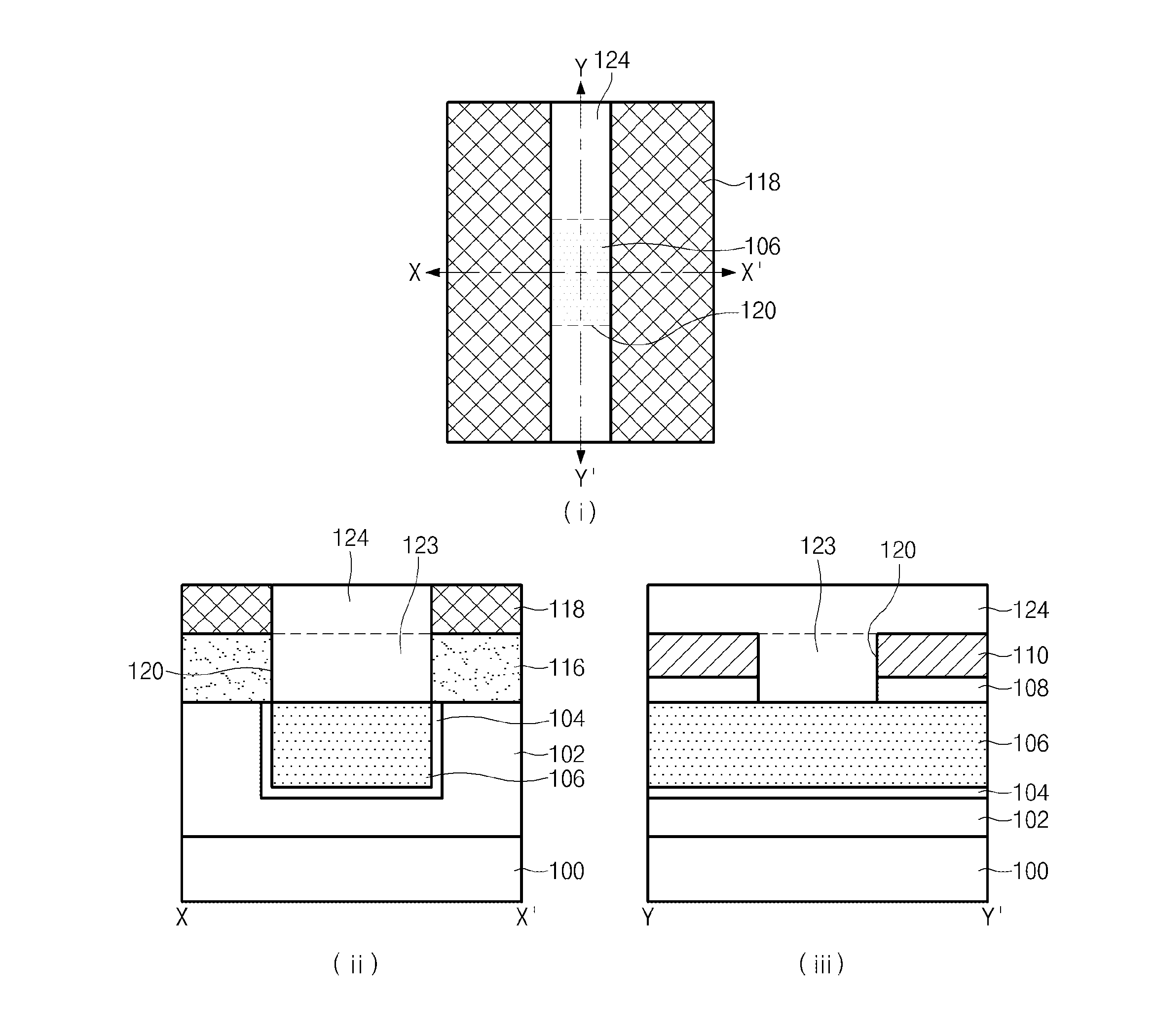
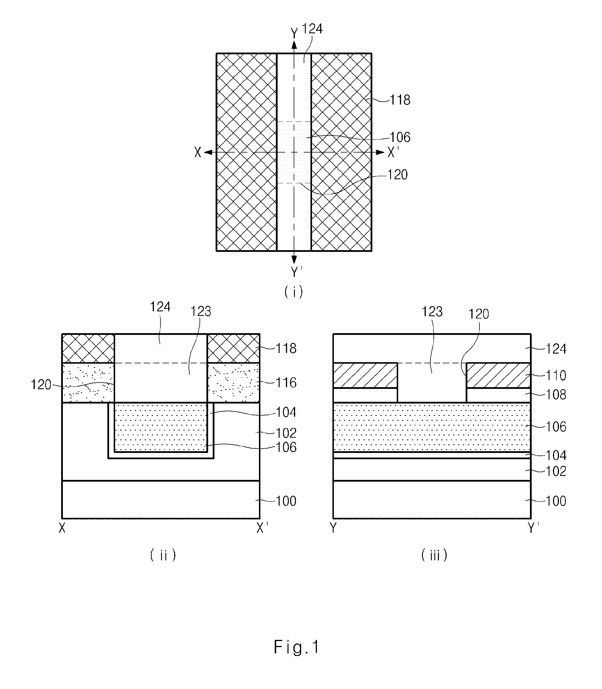
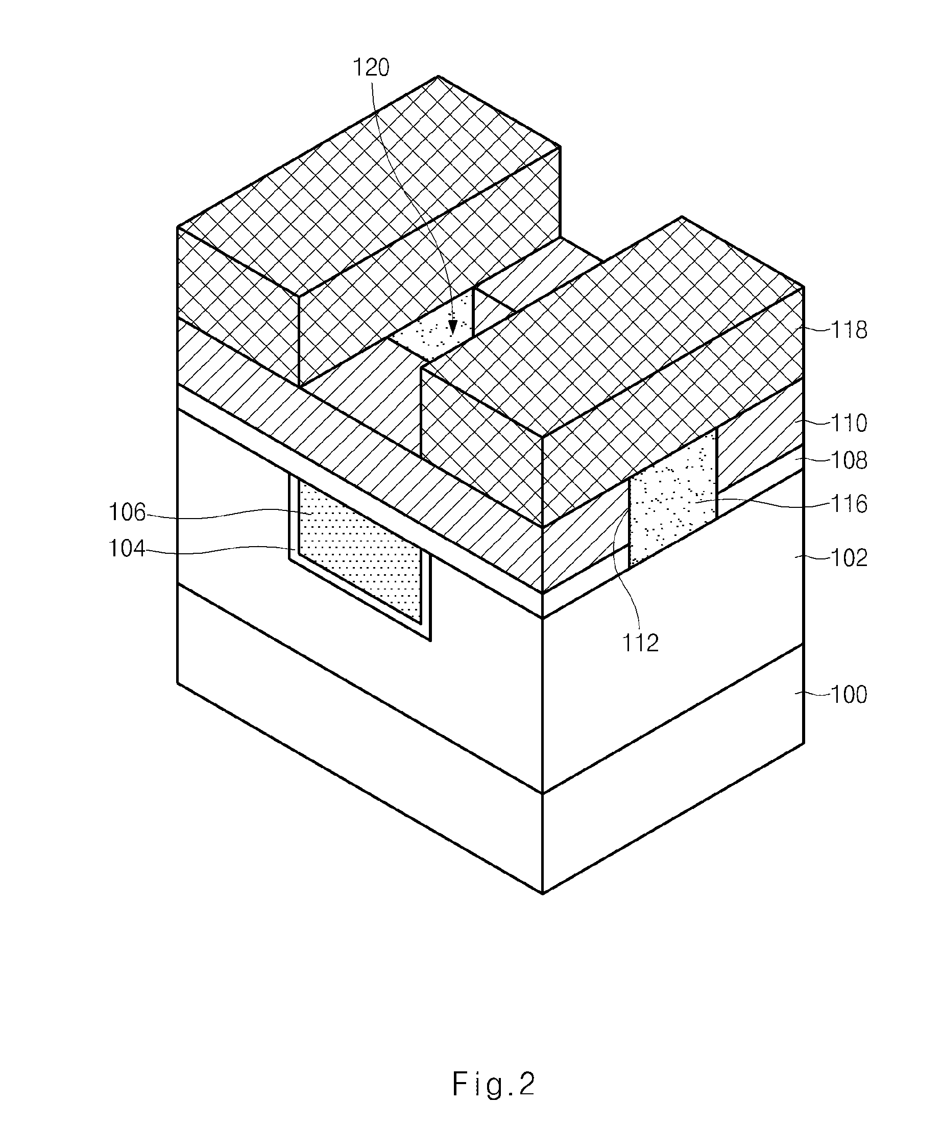
[0036]FIGS. 1(i) to 1(iii) illustrate a semiconductor device according to an embodiment of the present invention. FIG. 1(i) is a plan view illustrating the semiconductor device according to an embodiment of the present invention. FIG. 1(ii) is a cross-sectional view illustrating the semiconductor device taken along the line x-x′ of FIG. 1(i). FIG. 1(iii) is a cross-sectional view illustrating the semiconductor device taken along the line y-y′ of FIG. 1(i). FIG. 2 is a perspective view illustrating a semiconductor device according to an embodiment of the present invention.

[0037]Referring to FIGS. 1 and 2, the semiconductor device according to an embodiment of the present invention includes an interlayer insulating layer 10...


PUM


Abstract

The semiconductor device comprises a metal line configured to be buried in an interlayer insulation layer formed over a semiconductor substrate, a first insulating pattern configured to be formed over the interlayer insulating layer and the first metal line so that the first metal line is exposed, a second insulating pattern configured to be buried between the first insulating patterns so that the first metal line is exposed, and a third insulating pattern configured to be formed over the first insulating pattern and the second insulating pattern so that the first metal line is exposed, thereby reducing the resistance of a contact plug, such that it operates at high speed and requires low power consumption.

Description

CROSS-REFERENCE TO RELATED APPLICATION[0001]The priority of Korean patent application No. 10-2010-00069141 filed on Jul. 16, 2010, the disclosure of which is hereby incorporated in its entirety by reference, is claimed.BACKGROUND OF THE INVENTION[0002]1. Field of the Invention[0003]Embodiments of the present invention relate to a semiconductor device and a method for forming the same, and more particularly to a semiconductor device including a contact plug and a method for forming the same.[0004]2. Background of the Invention[0005]In a manufacturing process of a semiconductor device, it is necessary to form a metal contact plug for electrically coupling a predetermined lower metal line to an upper metal line. However, in recent times, as the semiconductor device is highly integrated and super-miniaturized, it is necessary to more precisely form a metal contact plug for interconnection between metal lines. In addition, as the demand of electrical characteristics and operation speed o...

Claims


Application Information

Patent Timeline
Patent Type & Authority Applications(United States)
IPC IPC(8): H01L23/522H01L21/306H01L21/768
CPCH01L21/76808H01L23/53223H01L23/53238H01L23/53266H01L23/5329H01L2924/0002H01L23/53295H01L2221/1031H01L2924/00
Inventor JANG, CHI HWAN
Owner SK HYNIX INC
Why Eureka
Try Eureka