Magnetic detection device

Active Publication Date: 2012-01-19
AICHI STEEL
View PDF0 Cites 24 Cited by
  • Summary
  • Abstract
  • Description
  • Claims
  • Application Information

AI Technical Summary

Benefits of technology

[0009]Furthermore, these MI elements 101, 102, 103 and the integrated circuit 200 have been connected with each other by what is called wire bonding. Therefore, additional space for wire bonding has been required and such a conventional magnetic detection device has been difficult to be reduced in size. Especially in respect to the Z-axis direction, the Z-axial MI element 103 is originally long and additionally wire bonded in the Z-axis direction. Therefore, such a magnetic detection device has been very difficult to be reduced in size in the Z-axis direction or thickness. Besides, since wire bonding needs to install wires one by one, a wire bonding step requires much longer time. Therefore, there is a limit in improving productivity of ma

Problems solved by technology

Nowadays, however, attention is focusing on a magneto-impedance element (appropriately abbreviated as an “MI element”), whic

Method used


Image

  • Magnetic detection device
  • Magnetic detection device
  • Magnetic detection device

Examples


Example

Embodiment 1

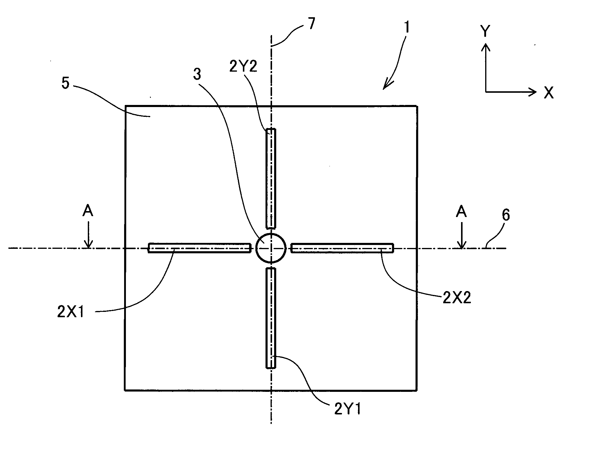
[0081]A three-dimensional magnetic detection device 1 according to Embodiment 1 is shown in FIG. 1. FIG. 1A is a plan view of the three-dimensional magnetic detection device 1 and FIG. 1B is a cross sectional view cut along the line A-A in FIG. 1A.

[0082]

[0083](1) The three-dimensional magnetic detection device 1 comprises four MI elements 2 for detecting geomagnetism (an external magnetic field), a rod-shaped soft magnetic body (a magnetic field direction changer) 3, a silicon substrate 4 having an integrated circuit 41 (including drive circuits) thereon, and an electrically insulating coating layer 5, and terminal holes (not shown) for respectively connecting terminals of the MI elements 2 and terminals of the integrated circuit 41. The four MI elements 2 comprise two X-axial MI elements 2X1, 2X2 (arbitrarily collectively referred to as “X-axial MI elements 2X”), and two Y-axial MI elements 2Y1, 2Y2 (arbitrarily collectively referred to as “Y-axial MI elements 2Y”).

[008...

Example

Embodiment 2

[0128]FIG. 8 shows a plan view of a three-dimensional magnetic detection device 20 in which arrangement of MI elements 2 is changed from that of the three-dimensional magnetic detection device 1 (FIG. 1). It should be noted that the same reference numerals will be used for convenience to refer to similar parts to those of the aforementioned three-dimensional magnetic detection device (hereinafter the same shall apply).

[0129]In the three-dimensional magnetic detection device 20, MI elements 2 are arranged on a square silicon substrate 4 so as to lie along diagonal lines at an angle of 45 degrees with respect to each side of the square. The MI elements 2 thus arranged can have a larger length with respect to a substrate of the same size. That is to say, length of the magnetosensitive bodies (amorphous wires or the like) and turns of detection coils can be increased and, as a result, output voltages can be increased.

Example

Embodiment 3

[0130]FIG. 9 shows a cross sectional view of a three-dimensional magnetic detection device 30 in which a soft magnetic body 33 which is shorter in a Z-axis direction than the soft magnetic body 3 is arranged at a different position from that of the soft magnetic body 3. That is to say, in the three-dimensional magnetic detection device 30, the shorter soft magnetic body 33 is placed on the electrically insulating coating layer 5 without being buried in the silicon substrate 34. With this arrangement, a process for forming a hole in the silicon substrate becomes unnecessary. Moreover, the degree of integration of electronic circuits on the silicon substrate 34 can be increased by the size of the hole. In this case, planer arrangement of the shorter soft magnetic body 33 is the same as that of the soft magnetic body 3 in the three-dimensional magnetic detection device 1, i.e., a center of the silicon substrate 4.


PUM


Abstract

A magnetic detection device of the present invention includes at least one pair of first magnetosensitive bodies each comprising a soft magnetic material extending in a first axis direction and being sensitive to an external magnetic field oriented in the first axis direction; and a magnetic field direction changer comprising a soft magnetic material and changing an external magnetic field oriented in a different axis direction from the first axis direction into a measurement magnetic field having a component in the first axis direction which can be detected by the at least one pair of first magnetosensitive bodies. With this magnetic detection device, the external magnetic field oriented in the different axis direction can be detected by way of the first magnetosensitive bodies. As a result, while attaining magnetic detection with high accuracy, the magnetic detection device can be reduced in size or thickness by omitting a magnetosensitive body extending long in the different axis direction.

Description

TECHNICAL FIELD[0001]The present invention relates to a magnetic detection device used for a direction sensor or the like and detecting magnetism by MI elements.BACKGROUND ART[0002]Conventionally, magnetism has been measured to find a direction or the like. For example, an electronic compass measures a three-dimensional magnetic vector in order to find a precise direction. In this case, the electronic compass requires a magnetic sensor which individually measures magnetic vectors oriented in three directions of X, Y and Z.[0003]A Hall element, an MR element or the like is employed as such a magnetic sensor. Nowadays, however, attention is focusing on a magneto-impedance element (appropriately abbreviated as an “MI element”), which is entirely different in structure and principle from such conventional elements and has an incomparably high sensitivity.[0004]An MI element uses magneto-impedance effect (abbreviated as “MI effect”), which is a phenomenon in which when a high frequency p...

Claims


Application Information

Patent Timeline
IPC IPC(8): G01R33/02
CPCG01C17/30G01R33/063G01R33/0206G01R33/02G01V3/40H10N50/00
Inventor HONKURA, YOSHINOBUYAMAMOTO, MICHIHARUHAMADA, NORIHIKOSHIMODE, AKIHIROKATO, MASAYUKI
Owner AICHI STEEL
Why Eureka
Try Eureka