High speed 3D multi touch sensitive device

a multi-touch, touch-sensitive technology, applied in the direction of optics, instruments, electric digital data processing, etc., can solve the problems of difficult to view the information presented on the display, unsatisfactory transparency of the touch-sensitive layer, and inefficient way of realising a touch-sensitive display, etc., to achieve the effect of reliable touch detection

Inactive Publication Date: 2012-01-19
INTEGRITOUCH DEVMENT
View PDF5 Cites 23 Cited by
  • Summary
  • Abstract
  • Description
  • Claims
  • Application Information

AI Technical Summary

Benefits of technology

[0015]An object of the present invention is to overcome the above described problems of the known technologies in regards to providing a touch sensor which is durable, that provides a reliable detection of touch on the display and even capable of detecting a finger in the vicinity of the display surface. The present invention is based on the understanding that a display is associated with specific physical characteristics which influence the reliability of the detection of a touch on the display.
[0016]Particular advantages of the present invention are reliability of the detection of a touch on the display, improved robustness of the touch sensor, the improved matching towards available display driver circuits, the increased resolution (especially in the direction of the z-axis) of a touch on the touch sensitive display, and the ability to detect and determine the position, direction of movement and speed of movement of a conducting object approaching the touch sensitive display.
[0017]A particular feature of the present invention relates to the provision of a touch sensor with a basic configuration making it possible to reliably detect a touch on the display without deforming the display or requiring specially adapted display driver circuitry, and also the capability to determine the position of a conducting object, and tracking it, in three dimensions, a x- and y-position on the touch sensitive display itself and a z-position in the vicinity of the touch sensitive display. By allowing for a high resolution three-dimensional tracking of objects using cost efficient touch displays, a whole new design space for future applications opens up.
[0018]The above objects, advantages and features together with numerous other objects, advantages and features, which will become evident from the detailed description below, are obtained according to a first aspect of the present invention by a touch sensor capable of determine at least one position of at least one conducting object with respect to a display device of said touch sensor, comprising said display device having a substrate on which substrate at least one display electrode is disposed for the display of a shape on the display device, an interface coupled to the at least one display electrode for receiving display data to the display device, a measuring circuit coupled to the at least one display electrode, switching means for connecting the interface to the at least one display electrode when the switching means is in a first state of operation and connecting the measuring circuit to the at least one display electrode when the switching means is in a second state of operation wherein the measuring circuit, when said switching means is in said second state of operation, is adapted to perform at least one measurement of the capacitive load of said at least one display electrode, wherein said measurement is performed by at a time instant, charging at least one capacitive load of said at least one display electrode by a predefined signal, wherein said charging results in at least one charging curve, determining the size of said at least one capacitive load of said at least one display electrode by measuring at least one rise time of said at least one charging curve, and calculating at least one position of said at least one conducting object, with respect to said display device, based on said determined size of the at least one capacitive load.

Problems solved by technology

Even though the separate touch sensitive layer makes it possible to enter data into the device in a crude way without the need for a keyboard, it is not an efficient way of realising a touch sensitive display since the transparency of the touch sensitive layer is not absolute, hence making it difficult to view the information presented on the display under certain circumstances.
The unsatisfactory transparency of the touch sensitive layer is even more noticeable when the display device is provided with back lighter or front lighter technology for making it possible to view the information on the display under poor lit conditions.
However, the solution according to U.S. Pat. No. 5,043,710 becomes complex due to the large amount of integrators needed for sensing a touch.
Moreover, for sensing a touch the front glass plate needs to be flexible making the display less durable and also very limited in terms of resolution in the direction of the z-axis.
In addition to this, the working life of the display is also decreased due to the repeated compressions of the liquid crystal in the display, which eventually will break the display cell chamber causing it to leak fluid or to suck in air.
And due to the fact this display need a physical force and contact to depress, it is impossible to detect or measure an object such as a finger advancing towards the display.
The LCD displays capability of detecting multiple touches at the same time on the display is very limited.
As will be disclosed below, the counter-electrode will act as a short-circuit between the electrodes on the front substrate thereby deteriorating the accuracy of the touch sensitive display in regard of where on the screen the touch is made.
Moreover, numerous stray-capacitances in the needed drive circuitry for the display will interfere with the capacitance measuring circuitry making it hard to determine where and if a touch is made.
Due to that the display cell gap distance usually is only fractions of the front or back glass thickness and to the common ground plane it will be almost impossible to get any resolution in the direction of the z-axis.
However, by arranging a conductive layer in front of the display element, the visibility of the display element is deteriorated.
Moreover, the conductive layer will be exposed to wear from users of the display, which implies that the endurance of the display will be insufficient for many applications.
Since there are no dielectric distance between the object touching the conducting layer it will be almost impossible to get any resolution in the direction of the z-axis.
Today gesture analysis is quite crude and often limited to comparing an entered two-dimensional signature (drawn on the surface of the touch sensitive display in plane spanned by the x- and the y-axis) with a stored version of the two-dimensional signature.
However, in the near future this level of security is not enough.

Method used


Image

  • High speed 3D multi touch sensitive device
  • High speed 3D multi touch sensitive device
  • High speed 3D multi touch sensitive device

Examples


Embodiment Construction

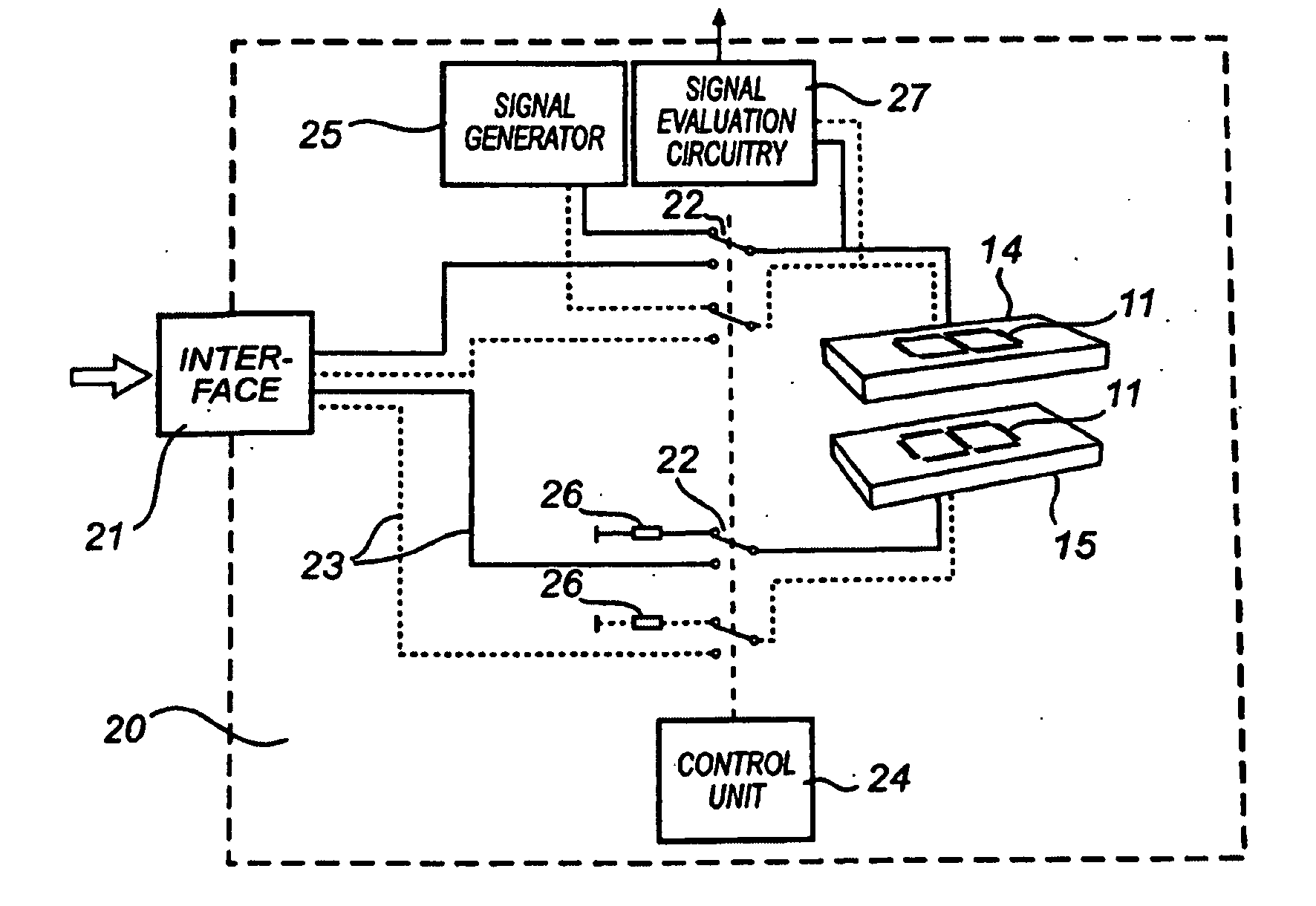
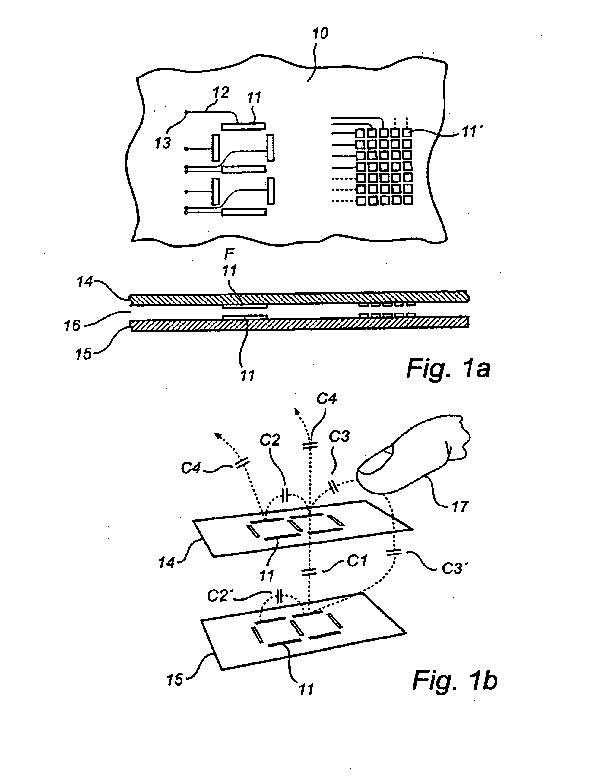
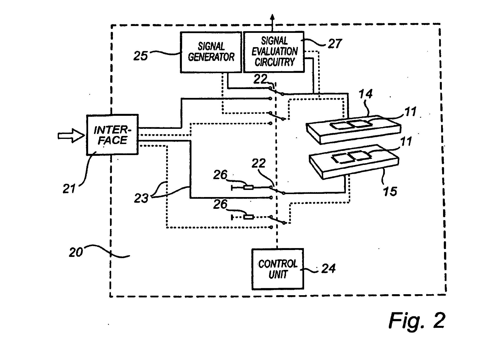
[0035]The most common display used today is the liquid crystal display (LCD) whose design and operation is well-known to the skilled person. Variants of the LCD display, e.g. Thin Film Transistor Displays (TFT) as well as other display techniques, such as Plasma Display Panels (PDP), Vacuum Fluorescent Displays (VFD), Ferroelectric Liquid Crystal displays (FLC), Surface stabilized cholesteric texture type (SSCT) displays, Organic Light Emitting Diode (OLED) displays, Electrical Paper Displays (EPD) or Electrical Ink Displays (EINK), and Liquid Crystal on Silicon (LCOS) displays are commonly used depending on the specific field of application. For the sake of simplicity the following text will disclose a touch sensitive display in form of a LCD, wherein a change in capacitance in the display is detected. The present invention is, however, not limited to such a display, but may be implemented on a display of any kind comprising at least one substrate on which at least one display elec...


PUM


Abstract

Disclosed are a touch sensor and a method for determining a position, in three dimensions, of a conducting object with respect to a display device of the touch sensor. The determination of the position of the conducting object is done by performing at least one measurement of the capacitive load of at least one display electrode of the display wherein the measurement is performed by charging the capacitive load of the at least one display electrode by a predefined signal. The charging results in at least one charging curve, from which the capacitive load of the at least one display electrode may be determined by measuring the rise time of the charging curve of the charging, and calculating the position of the at least one conducting object, with respect to said display device based on the determined capacitive load.

Description

[0001]This is a continuation-in-part application of U.S. patent application Ser. No. 12 / 659,772, filed Mar. 22, 2010, which is a continuation application of U.S. patent application Ser. No. 10 / 575,622, filed Apr. 13, 2006, now U.S. Pat. No. 7,705,834, which claims priority from Swedish Patent Application No. 0302711-7, filed Oct. 13, 2003, and the benefit of U.S. Provisional Application No. 60 / 516,314, filed Nov. 3, 2003, the entire contents of all of which are incorporated herein by reference.TECHNICAL FIELD[0002]The present invention relates in general to the field of display devices, and more particularly, to touch sensitive display devices with high input sensitivity.BACKGROUND[0003]Electrical equipment from various fields of application, e.g. mobile telephones, personal digital assistants (PDA), and industrial control equipment often use a display device of some sort for providing the operator of the device with information. In simpler applications the display device is a one-w...

Claims


Application Information

Patent Timeline
Patent Type & Authority Applications(United States)
IPC IPC(8): G06F3/044
CPCG02F1/13338G02F1/1343G09G3/18G06F3/044G06F2203/04101G06F3/0412G06F3/0443
Inventor SWEDIN, ANDERS
Owner INTEGRITOUCH DEVMENT
Why Eureka
Try Eureka