Image display apparatus

a technology of image display and display device, which is applied in the direction of static indicating device, cathode-ray/electron beam tube circuit element, instruments, etc., can solve the problems of high voltage not being supplied to the part of the power supply line beyond the disconnected part, and the appearance of a dark line, so as to facilitate the prevention of image deterioration, less streaking, and favorable image

Inactive Publication Date: 2012-01-19
CANON KK
View PDF2 Cites 128 Cited by
  • Summary
  • Abstract
  • Description
  • Claims
  • Application Information

AI Technical Summary

Benefits of technology

[0015]According to the present invention, since the condition of R2<R1all is met, even in case that a line disconnection occurs in the first resistive element, an image with no extreme dark line generated can be provided, and furthermore, destruction of the second resistive element is hard to occur upon occurrence of a discharge. Furthermore, since the condition of 0.1×R1<R2 is met, a favorable image with less streaking can be provided.
[0016]The present invention enables provision of an image display apparatus that facilitates prevention of image deterioration resulting from a dark line or streaking while suppressing generation of an abnormal current due to a discharge, as well as prevention of destruction of resistor members.

Problems solved by technology

In such image display apparatus, the space between the rear plate and the face plate is very small and a high voltage is applied between the rear plate and the face plate for acceleration of the electrons, and causing a problem of what countermeasures to be taken for discharge.
Meanwhile, where one end of each power supply line is terminated in isolation without connection to another power supply line or a common electrode, if a power supply line is disconnected, a high voltage cannot be supplied to the part of the power supply line beyond the disconnected part.
Consequently, light emitting members not supplied with the high voltage cannot emit light, resulting in appearance of a dark line, which is a significant image defect.
Firstly, if resistances of the resistor members connecting the ends of the power supply lines on each of the opposite sides thereof are excessively high, the degree of image deterioration caused by a dark line resulting from line disconnection cannot be lessened. Even where the ends of the power supply lines are connected on each of the opposite sides thereof, if a part whose resistance value is extremely high exits at a position somewhere in the route of the connection, a voltage drop is caused by a current emitted from the rear plate. Here, in the present specification, “emitted current” is used as a term referring to a flow of electrons, and the direction of an emitted current is opposite to the direction of a current in the ordinary sense.
Secondly, where the resistances of the resistor members are excessively high, the potential difference between opposite ends of a relevant resistor member becomes large upon occurrence of a discharge, which may result in destruction of the resistor member. When a discharge occurs between the face plate and the rear plate, a voltage drop occurs in the resistor members according to a current flowing onto the face plate and the resistance values in the route in which the current flows. In such case, if only the resistor members have an extremely high resistance value, the potential difference between the opposite ends of the resistor members becomes large and thus, a secondary discharge may occur, which leads to irreversible deviation of the electrical characteristics of the resistor members from desired characteristics, resulting in image deterioration.
Thirdly, contrarily, if the resistor members have an extremely low resistance value, image quality deterioration called crosstalk or streaking may occur when a particular figure is displayed. Especially, in an FED in which line sequential driving is performed, the direction in which the resistive element is divided into the power supply lines (the direction in which the power supply lines extend) is perpendicular to scanning lines, image quality deterioration easily grows.

Method used


Image

  • Image display apparatus
  • Image display apparatus
  • Image display apparatus

Examples


example 1

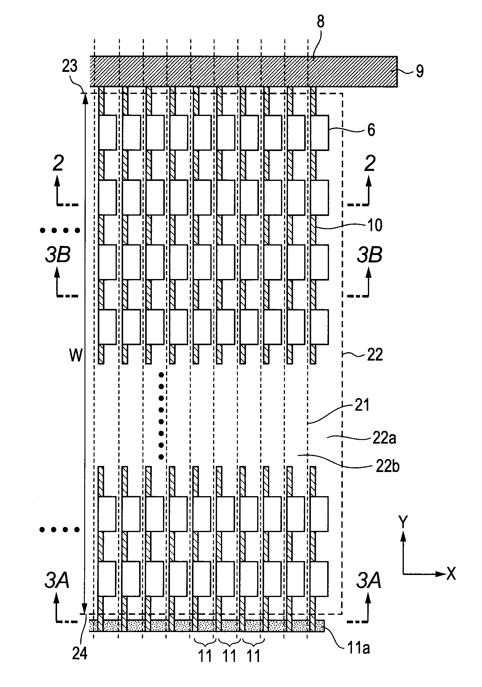
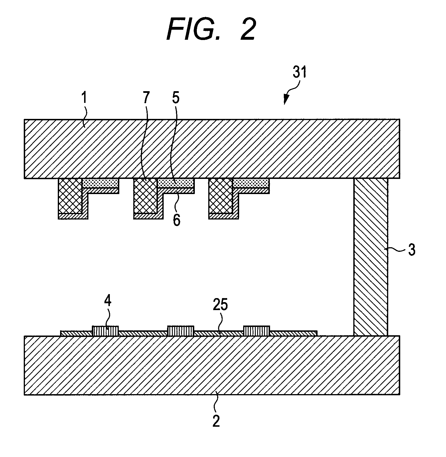
[0067]A face plate with the configuration illustrated in FIG. 1 was fabricated according to the process described below. An X direction and a Y direction in the following description are those illustrated in FIG. 1.

[0068]A glass substrate with a thickness of 2.8 mm (PD200 manufactured by Asahi Glass Co., Ltd.) as a substrate for the face plate 1, and a light-shielding layer (NP-7803D manufactured by Noritake Kizai Co., Ltd.) was formed on the glass substrate. Next, ribs 7 are formed by a photolithographic method, and phosphors 5 for RGB were applied between the ribs 7 and subjected to firing. Subsequently, an island-shaped anode layer 6 was formed on the phosphors 5 by a vacuum vapor deposition method. Finally, first resistive elements 10 and second resistive elements 11 were formed in this order by a photolithographic method, respectively. The pixel pitch was 900 μm and the width in the X direction of each of RGB was 300 μm. The number of pixels are 100×100 pixels, i.e., 300×100 in...

example 2

[0072]A face plate with the configuration illustrated in FIG. 4 was fabricated by the following process. An X direction and a Y direction in the below description correspond to those illustrated in FIG. 4.

[0073]A black paste (containing a black pigment and a glass frit) was subjected to screen printing on a surface of a cleansed glass substrate (PD200 manufactured by Asahi Glass Co., Ltd.) with a thickness of 1.8 mm so as to form a pattern of openings in a matrix on the substrate. In the opening pattern, the size of each opening has 150 μm (X direction)×300 μm (Y direction), the X-direction pitch of the openings was 200 μm, the Y-direction pitch of the openings was 600 μm, and openings corresponding to 300 sub-pixels in the X direction and 100 sub-pixels in the Y direction were formed. The substrate was dried at 120° C., and then fired at 550° C. to form a black matrix with a thickness of 5 μm (not illustrated).

[0074]Next, a plurality of ribs 7 were formed in stripes. A photosensiti...


PUM


Abstract

An image display apparatus comprises a face plate including a common electrode extending in an outside of an image region along a one side of the image region, n first resistor members connected to the common electrode and connected to each of anodes in the divisional regions corresponding thereto, and a second resistor member connecting between one and the other of the first resistor members. R1 is an average resistance value of each first resistor member per length of one pixel including at least one of the light emitting members. R1all is a resistance value of each first resistor member for a total length in the image region. R2 is a resistance value of the second resistor member. And, a relationship of 0.1×R1<R2<R1all is met.

Description

BACKGROUND OF THE INVENTION[0001]1. Field of the Invention[0002]The present invention relates to an image display apparatus, and specifically relates to a configuration of resistor members provided on a face plate.[0003]2. Description of the Related Art[0004]Conventionally, an image display apparatus including a rear plate on which a plurality of electron-emitting sources are formed and a face plate on which light emitting members that emit light responsive to collision with electrons emitted from the electron-emitting sources and accelerated are formed has been known. In such image display apparatus, the space between the rear plate and the face plate is very small and a high voltage is applied between the rear plate and the face plate for acceleration of the electrons, and causing a problem of what countermeasures to be taken for discharge.[0005]Japanese Patent Application Laid-Open No. 2005-251530 discloses an image display apparatus in which a anode is divided in a row direction...

Claims


Application Information

Patent Timeline
Patent Type & Authority Applications(United States)
IPC IPC(8): G09G5/00
CPCH01J29/085H01J29/96H01J2329/96H01J2329/08H01J2329/28H01J31/127
Inventor INOUE, YUKIHIROONISHI, TOMOYA
Owner CANON KK
Why Eureka
Try Eureka