Support structures for various apparatuses including opto-electrical apparatuses

a technology of supporting structure and apparatus, applied in the direction of chemistry apparatus and processes, transportation and packaging, coatings, etc., can solve the problems of affecting the relative the manufacturing process and after-production use environment can be comparatively harsh and detrimental to the relatively delicate characteristics and features of thin film devices, and the structure of the device is supplied. structural and mechanical integrity, greater flexibility characteristics, and the effect of increasing the rigidity

Inactive Publication Date: 2012-01-19
ALTA DEVICES INC
View PDF5 Cites 9 Cited by
  • Summary
  • Abstract
  • Description
  • Claims
  • Application Information

AI Technical Summary

Benefits of technology

[0005]Present embodiments generally relate to support structures for thin film components and methods for fabricating the support structures. In one embodiment, an apparatus comprises a device structure including portions of a device; and a support structure coupled to the device structure; wherein the support structure supplements features of the device structure. The support structure can include a metal component coupled to the device structure. The support structure can include a non-metal component coupled to the metal component. The support component can supplement structural and mechanical integrity of the device structure. The support component can supplement functional operations of the device structure. In one embodiment, the metal component includes at least one layer of metal material. In one embodiment, the non-metal component includes at least one layer of non-metal material (e.g., polymeric material, etc.). In one exemplary implementation, the metal component can have greater stiffness characteristics with respect to the device structure and the non-metal component can have greater flexibility characteristics with respect to the metal layer component. The support structure can be configured to reflect light towards the device structure. The support structure can also be configured to conduct electricity from the device structure.

Problems solved by technology

Manufacturing and utilizing thin film devices can be very complex and complicated.
Thin film components can be very difficult to manufacture and handle since the films are typically very fragile and have narrow dimensions.
The manufacturing processes and after manufacture use environments can be comparatively harsh and detrimental to the relatively delicate characteristics and features of thin film devices.
The thin films can be very susceptible to physical damage (e.g., cracking and breaking under very small forces, etc.).
Thin film devices can include relatively brittle components or characteristics that do not permit much or any deformation before structural or mechanical failure.
Such failures can adversely affect production yields and in field use effectiveness of the thin film components.

Method used


Image

  • Support structures for various apparatuses including opto-electrical apparatuses
  • Support structures for various apparatuses including opto-electrical apparatuses
  • Support structures for various apparatuses including opto-electrical apparatuses

Examples


example 1

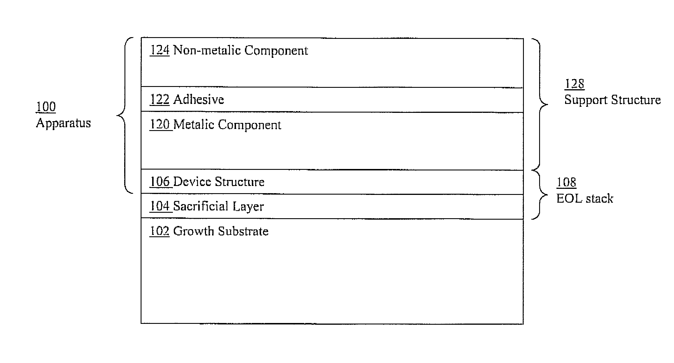
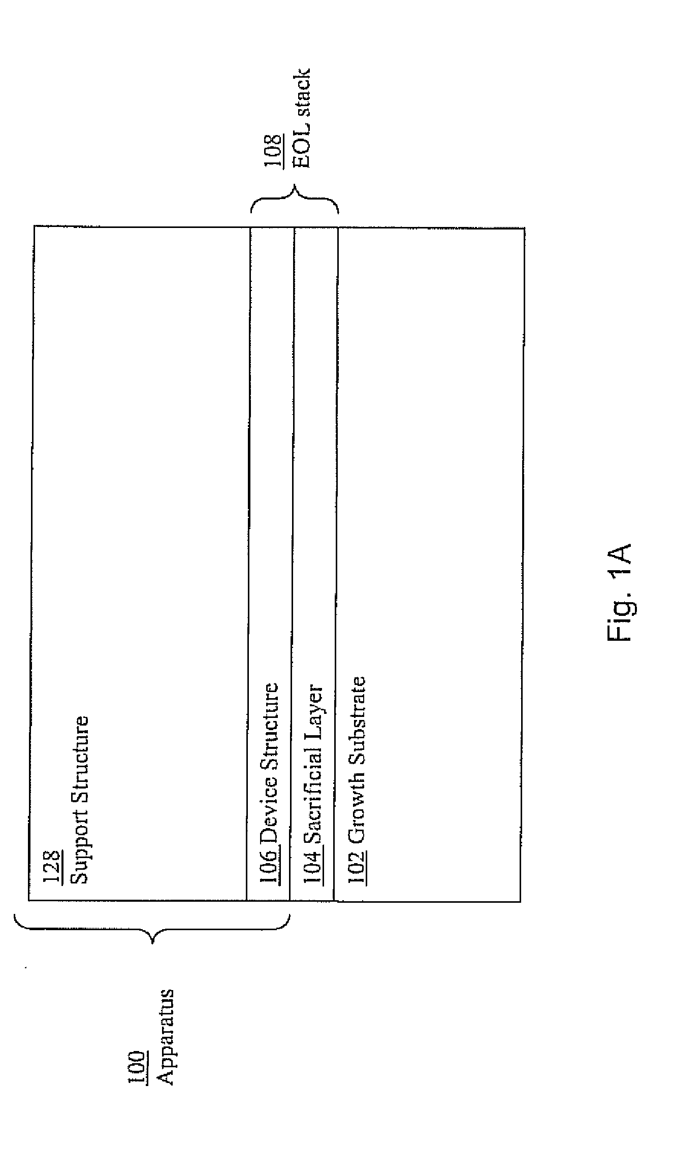
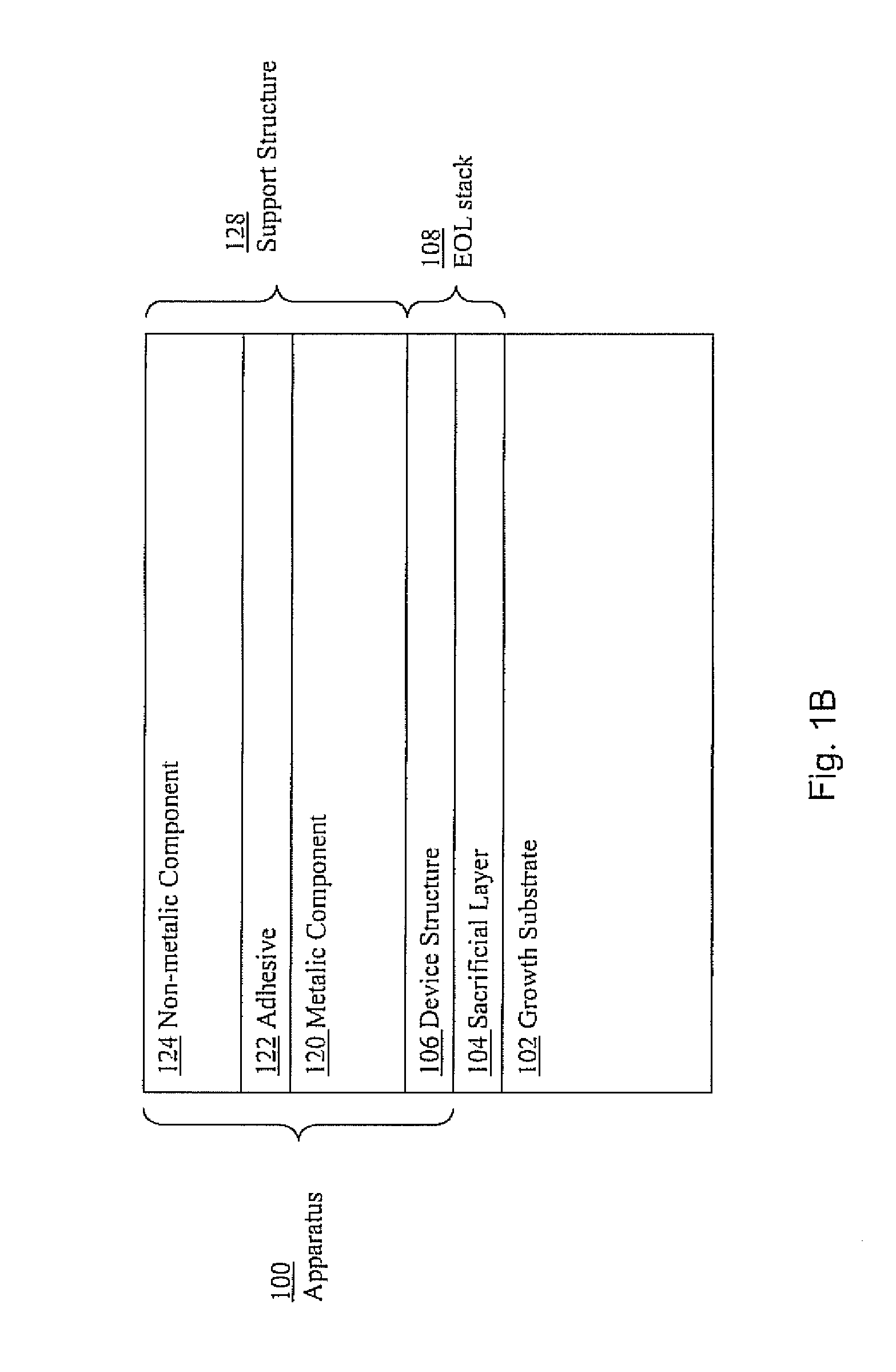
[0085]The support structure contains a metallic support layer of copper foil (e.g., thickness of about 5 μm) disposed on the device structure, an adhesion layer containing an acrylic PSA (e.g., thickness of about 40 μm) or a layer of EVA (e.g., thickness of about 30 μm) disposed on the metallic support layer, and a laminated support layer deposited containing a polyethylene terephthalate polyester (e.g., thickness of about 60 μm).

example 2

[0086]The support structure contains a metallic support layer of copper foil (e.g., thickness of about 5 μm) disposed on the device structure, an adhesion layer containing an acrylic PSA (e.g., thickness of about 40 μm) or a layer of EVA (e.g., thickness of about 30 μm) disposed on the metallic support layer, and a laminated support layer deposited containing a polyethylene terephthalate polyester (e.g., thickness of about 100 μm).

example 3

[0087]The support structure contains a metallic support layer of copper foil (e.g., thickness of about 5 μm) disposed on the device structure, an adhesion layer containing an acrylic PSA (e.g., thickness of about 40 μm) or a layer of EVA (e.g., thickness of about 30 μm) disposed on the metallic support layer, and a laminated support layer deposited containing a polyethylene terephthalate polyester (e.g., thickness of about 200 μm).


PUM

PropertyMeasurementUnit
etch rateaaaaaaaaaa
etch rateaaaaaaaaaa
etch rateaaaaaaaaaa

Abstract

Present embodiments generally relate to support structures for thin film components and methods for fabricating the support structures. In one embodiment, an apparatus comprises a device structure including portions of an electronic device; a support structure coupled to the device structure; wherein the support structure supplements features of the device structure and the support structure includes: a metal component coupled to the device structure; and a non-metal component coupled to the metal component. The support component can supplement structural and mechanical integrity of the device structure and functional operations of the device structure. In one embodiment, the metal component includes at least one layer of metal material and the non-metal component includes at least one layer of non metal material (e.g., polymeric material, etc.). The metal component can have greater stiffness characteristics with respect to the device structure and the non-metal component can have greater flexibility characteristics with respect to the metal layer component. The support structure can be configured to reflect light towards the device structure. The support structure can also be configured to conduct electricity from the device structure.

Description

RELATED APPLICATIONS[0001]The present Application claims the benefit of and priority to Provisional Application 61 / 297,692 (Attorney Docket Number ALTA / 0022L) entitled “Laminated Metallic Support Films For Epitaxial Lift Off Stacks” filed Jan. 22, 2010 and Provisional Application 61 / 297,702 (Attorney Docket Number ALTA / 0022L02) entitled “Methods For Forming Epitaxial Lift Off Stacks Containing Laminated Metallic Support Films” filed Jan. 22, 2010, which are both incorporated herein by reference.FIELD OF THE INVENTION[0002]Embodiments of the invention generally relate to the fabrication and use of various apparatuses (e.g., including photovoltaic, opto-electric, optical, semiconductor, electronic thin film devices, etc.) and more, particularly in some embodiments configuration and fabrication of support structures associated with the apparatuses.BACKGROUND OF THE INVENTION[0003]Various devices and circuits are often utilized in a number of applications to achieve advantageous results...

Claims


Application Information

Patent Timeline
Patent Type & Authority Applications(United States)
IPC IPC(8): B32B7/02B05D3/00B05D5/10B32B15/04
CPCH01L21/6835H01L21/7806H01L31/0392Y10T428/24942H01L2221/6835H01L2221/68363Y02E10/50H01L31/1892Y10T428/31678
Inventor HE, GANGGMITTER, THOMAS J.ARCHER, MELISSA
Owner ALTA DEVICES INC
Why Eureka
Try Eureka