Microelectronic elements with rear contacts connected with via first or via middle structures

a microelectronic element and rear contact technology, applied in the direction of semiconductor devices, semiconductor/solid-state device details, electrical apparatus, etc., can solve the problems of increasing the amount of silicon and increasing the cost of each chip

Active Publication Date: 2012-01-26
TESSERA INC
View PDF7 Cites 219 Cited by
  • Summary
  • Abstract
  • Description
  • Claims
  • Application Information

AI Technical Summary

Benefits of technology

[0041]FIG. 1 is a sectional view illustrating a stage in a method of fabricating a microelectronic unit in accordance with an embodiment of the invention.

Problems solved by technology

Such a reduction in the available space on the first face that can be used for active circuitry may increase the amount of silicon required to produce each semiconductor chip, thereby potentially increasing the cost of each chip.

Method used


Image

  • Microelectronic elements with rear contacts connected with via first or via middle structures
  • Microelectronic elements with rear contacts connected with via first or via middle structures
  • Microelectronic elements with rear contacts connected with via first or via middle structures

Examples


Embodiment Construction

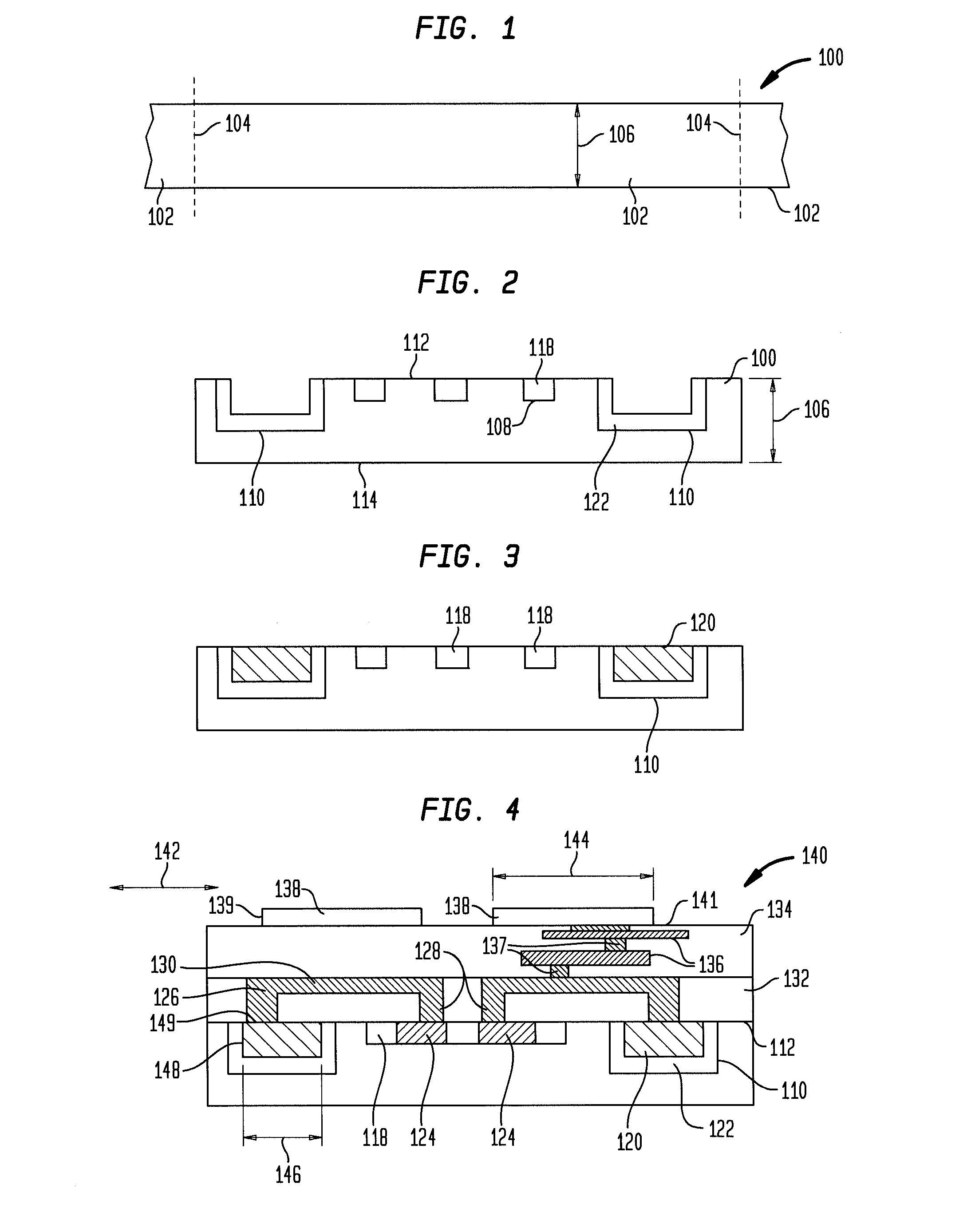
[0069]A monocrystalline semiconductor substrate, e.g., an intact wafer 100 or a portion of a wafer, is shown in FIG. 1. The wafer or wafer portion 100 is shown having a plurality of individual regions 102 which are attached to one another at peripheral edges 104 of each region 102. Through processing as further described, the regions 102 can become individual microelectronic elements, e.g., integrated circuit chips. Unless otherwise provided, processing as further described below is performed on a wafer or wafer portion which includes a plurality of regions attached to each other in this manner, either being referred to hereinafter as a “wafer”. Initially, the wafer 100 has a thickness 106 of several hundred microns. The wafer can consist essentially of silicon or a compound semiconductor material, for example, a III-V semiconductor compound such as gallium arsenide (GaAs) and the like, or a II-VI semiconductor compound.

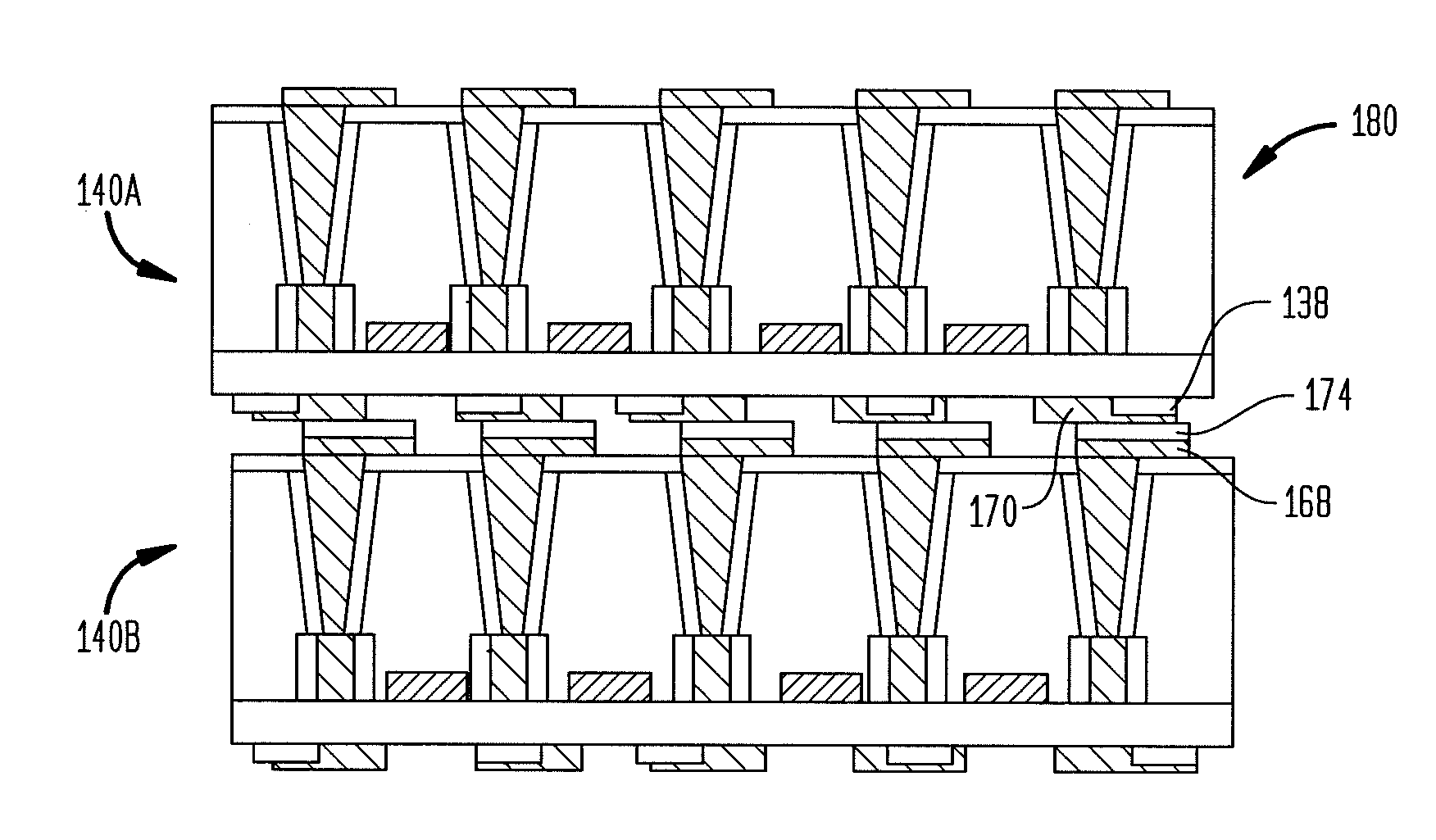
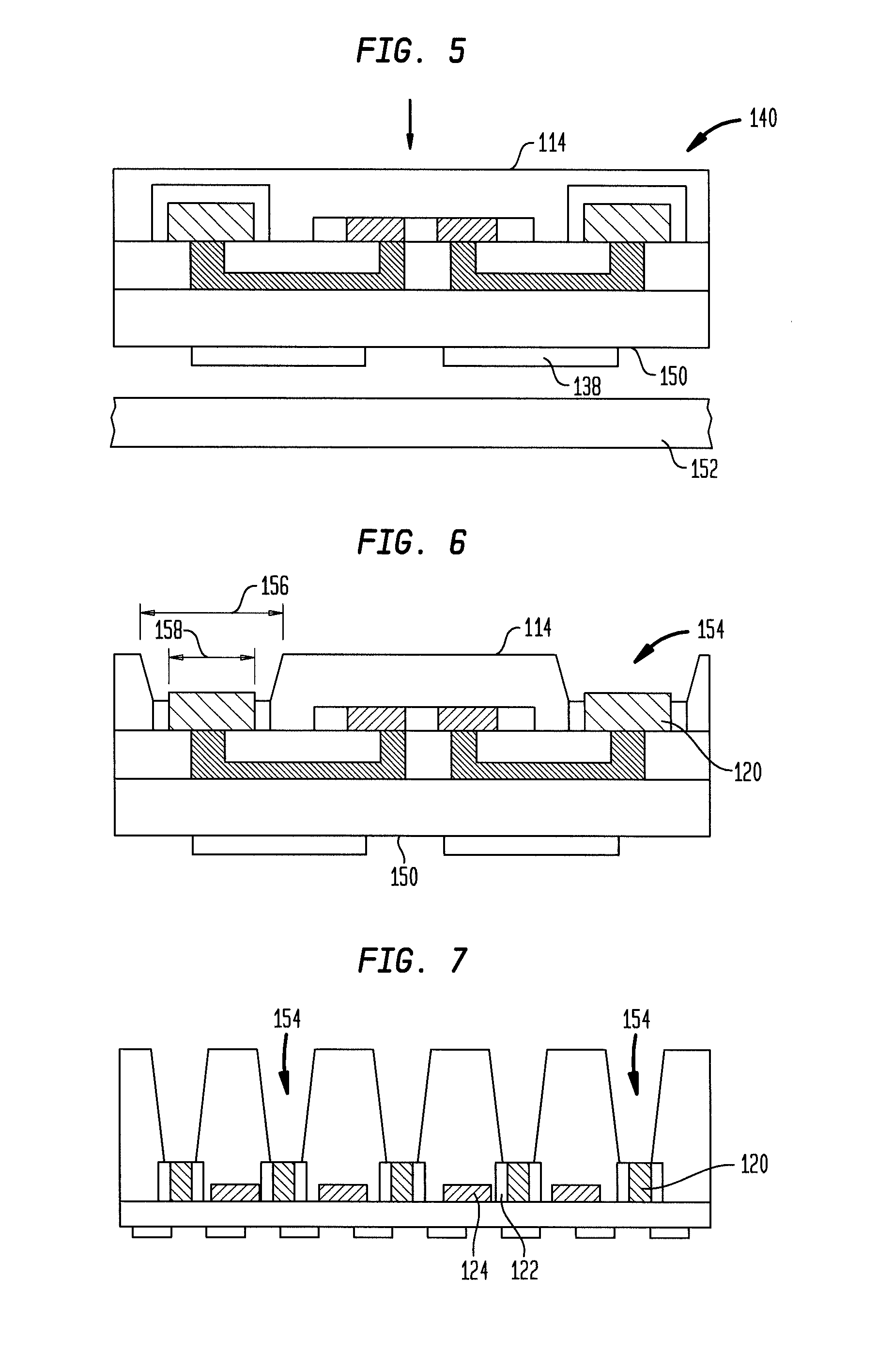
[0070]A “via first” flow will now be described with reference t...


PUM


Abstract

A microelectronic unit includes a microelectronic element, e.g., an integrated circuit chip, having a semiconductor region of monocrystalline form. The semiconductor region has a front surface extending in a first direction, an active circuit element adjacent the front surface, a rear surface remote from the front surface, and a conductive via which extends towards the rear surface. The conductive via can be insulated from the semiconductor region by an inorganic dielectric layer. An opening can extend from the rear surface partially through a thickness of the semiconductor region, with the opening and the conductive via having respective widths in the first direction. The width of the opening may be greater than the width of the conductive via where the opening meets the conductive via. A rear contact can be electrically connected to the conductive via and exposed at the rear surface for electrical connection with an external circuit element, such as another like microelectronic unit, a microelectronic package, or a circuit panel.

Description

BACKGROUND OF THE INVENTION[0001]The present invention relates to packaging of microelectronic devices, especially the packaging of semiconductor devices.[0002]Microelectronic devices generally comprise a thin slab of a semiconductor material, such as silicon or gallium arsenide, commonly called a die or a semiconductor chip. Semiconductor chips are commonly provided as individual, prepackaged units. In some unit designs, the semiconductor chip is mounted to a substrate or chip carrier, which is in turn mounted on a circuit panel, such as a printed circuit board.[0003]The active circuitry is fabricated in a first face of the semiconductor chip (e.g., a front surface). To facilitate electrical connection to the active circuitry, the chip is provided with bond pads on the same face. The bond pads are typically placed in a regular array either around the edges of the die or, for many memory devices, in the die center. The bond pads are generally made of a conductive metal, such as copp...

Claims


Application Information

Patent Timeline
Patent Type & Authority Applications(United States)
IPC IPC(8): H01L23/528H01L21/768
CPCH01L21/76898H01L23/481H01L25/0657H01L2924/0002H01L2924/00H01L24/05H01L24/06H01L24/16H01L2224/02372H01L2224/02375H01L2224/02377H01L2224/0401H01L2224/05548H01L2224/06181H01L2224/13024H01L2224/131H01L2224/13111H01L2224/133H01L2224/16146H01L2224/16227H01L2224/17181H01L2224/81801H01L2224/8182H01L2224/94H01L2224/1329H01L2224/8185H01L2224/06166H01L2924/014H01L2924/00014H01L2224/03H01L2224/81H01L25/07H01L21/00H01L25/065
Inventor OGANESIAN, VAGEHABA, BELGACEMMOHAMMED, ILYASMITCHELL, CRAIGSAVALIA, PIYUSH
Owner TESSERA INC
Why Eureka
Try Eureka