Microelectronic elements with post-assembly planarization

a technology of post-assembly and microelectronic elements, applied in the direction of basic electric elements, solid-state devices, electrical apparatus construction details, etc., can solve the problems of complexity, cost, thickness and testability of conventional stacked packages,

Active Publication Date: 2012-01-26
TESSERA INC
View PDF27 Cites 279 Cited by
  • Summary
  • Abstract
  • Description
  • Claims
  • Application Information

AI Technical Summary

Benefits of technology

[0041]Further aspects of the invention provide systems which incorporate microelectronic structures according to the foregoing aspects of the invention, composite chips according to the foregoing aspects of the invention, or both in conjunction with other electronic devices. For example, the system may be disposed in a single housing, which may be a portable housing. Systems according to preferred embodiments in this aspect of the invention may be more compact than comparable conventional systems.

Problems solved by technology

However, conventional stacked packages have disadvantages of complexity, cost, thickness and testability.

Method used


Image

  • Microelectronic elements with post-assembly planarization
  • Microelectronic elements with post-assembly planarization
  • Microelectronic elements with post-assembly planarization

Examples


Embodiment Construction

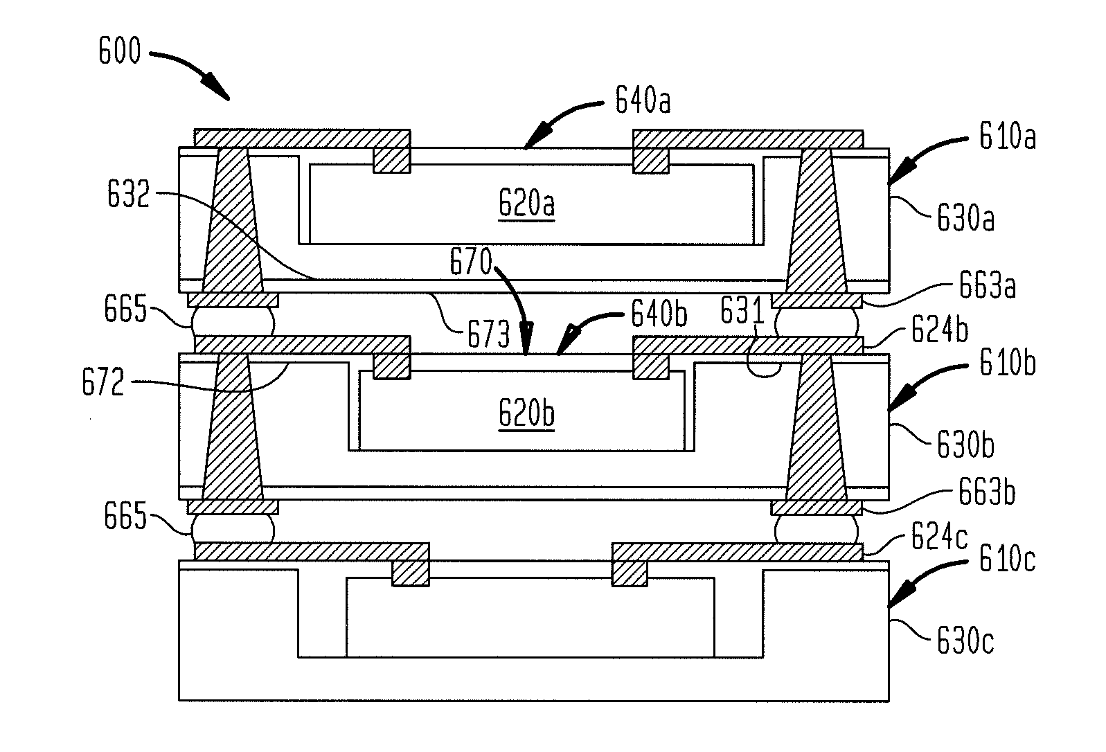
[0078]In the embodiments shown and described herein, microelectronic units can be planarized. Planarized microelectronic units can advantageously be incorporated in stacked assemblies. Reducing the number of different sizes of microelectronic units can also facilitate stacking of the microelectronic units.

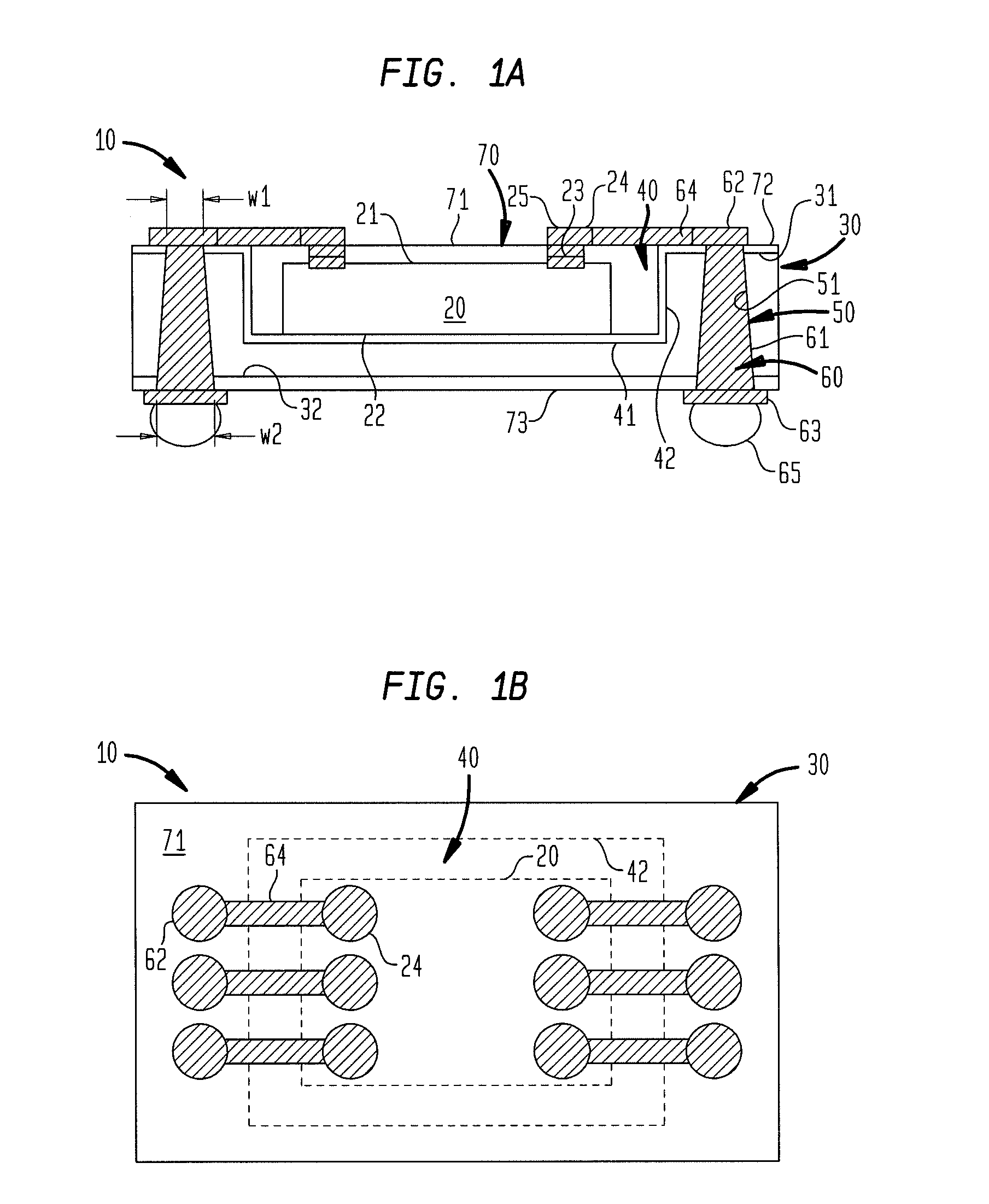
[0079]FIGS. 1A and 1B are a sectional view and a corresponding top-down plan view illustrating a packaged chip and chip carrier assembly in accordance with an embodiment of the invention. As illustrated in FIGS. 1A and 1B, a microelectronic unit 10 includes a microelectronic element 20 mounted to a carrier structure 30.

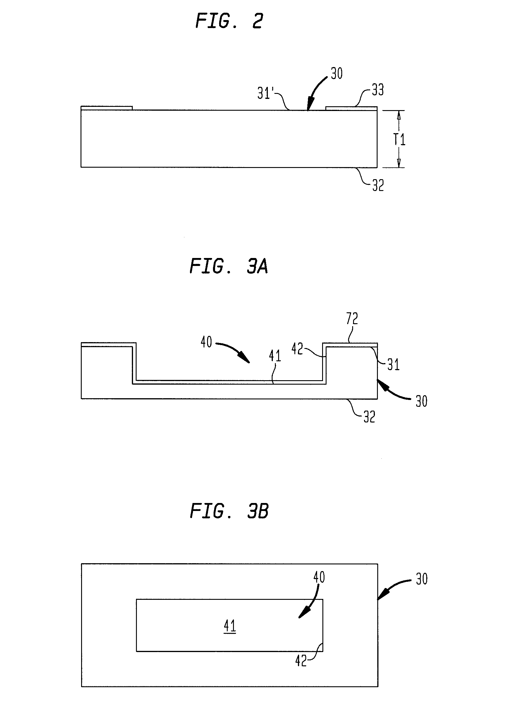
[0080]The microelectronic element 20 can include a semiconductor substrate, made for example from silicon, in which one or a plurality of semiconductor devices (e.g., transistors, diodes, etc.) is disposed in an active semiconductor region thereof located at and / or below the top surface 21. The thickness of the microelectronic element 20 between the top surface 21 an...


PUM

PropertyMeasurementUnit
thickaaaaaaaaaa
thicknessaaaaaaaaaa
angleaaaaaaaaaa

Abstract

A microelectronic unit includes a carrier structure having a front surface, a rear surface remote from the front surface, and a recess having an opening at the front surface and an inner surface located below the front surface of the carrier structure. The microelectronic unit can include a microelectronic element having a bottom surface adjacent the inner surface, a top surface remote from the bottom surface, and a plurality of contacts at the top surface. The microelectronic element can include terminals electrically connected with the contacts of the microelectronic element. The microelectronic unit can include a dielectric region contacting at least the top surface of the microelectronic element. The dielectric region can have a planar surface located coplanar with or above the front surface of the carrier structure. The terminals can be exposed at the surface of the dielectric region for interconnection with an external element.

Description

BACKGROUND OF THE INVENTION[0001]The present invention relates to packaging of microelectronic devices, especially the packaging of semiconductor devices. The present invention also relates to stacked microelectronic packages including stacked microelectronic packages fabricated at the wafer level and to methods of making such packages.[0002]Microelectronic elements generally comprise a thin slab of a semiconductor material, such as silicon or gallium arsenide, commonly called a die or a semiconductor chip. Semiconductor chips are commonly provided as individual, prepackaged units. The active circuitry is fabricated in a first face of the semiconductor chip (e.g., a front surface). To facilitate electrical connection to the active circuitry, the chip is provided with bond pads on the same face. The bond pads are typically placed in a regular array either around the edges of the die or, for many memory devices, in the die center. The bond pads are generally made of a conductive metal...

Claims


Application Information

Patent Timeline
Patent Type & Authority Applications(United States)
IPC IPC(8): H05K7/20H05K7/02H05K13/00
CPCH01L23/13H01L2924/01322H01L23/49827H01L23/4985H01L23/5389H01L24/24H01L24/25H01L24/82H01L25/105H01L25/50H01L2224/24227H01L2224/97H01L2225/1058H01L2924/01013H01L2924/01029H01L2924/01032H01L2924/01049H01L2924/01061H01L2924/01079H01L2924/01082H01L2924/15153H01L2924/15165H01L23/3128Y10T29/49002H01L2924/07811H01L2924/10253H01L24/18H01L2924/014H01L25/16H01L2225/1029H01L2225/1052H01L24/19H01L2924/01005H01L2924/01006H01L2924/01023H01L2924/01033H01L2924/01047H01L2224/81H01L2924/00H01L24/97H01L2224/12105H01L2224/04105H01L2224/24247H01L2224/32245H01L2224/32225H01L2224/73267H01L2924/12042H01L2924/14H01L2224/82H01L2224/83H01L2224/16227H01L2224/16235H01L2224/92244H01L2225/1023H01L2225/1035H01L2225/1041H01L2924/15156H01L2924/15192H01L2924/15311H01L2924/15313H01L2924/15331H01L2924/157H01L2924/15788H01L2924/18161H01L21/76819H01L21/76877H01L24/20H01L25/117
Inventor OGANESIAN, VAGEHABA, BELGACEMMITCHELL, CRAIGMOHAMMED, ILYASSAVALIA, PIYUSH
Owner TESSERA INC
Why Eureka
Try Eureka