Sensor device and manufacturing method

Inactive Publication Date: 2012-02-02
NXP BV
View PDF6 Cites 10 Cited by
  • Summary
  • Abstract
  • Description
  • Claims
  • Application Information

AI Technical Summary

Benefits of technology

[0017]Hence, the method of the present invention leads to a sensor device in which the sensing electrode and the counter electrode, as well as the sample chamber comprising these electrodes are integrated in the BEOL metallization stack without requiring non-standard semiconductor processing steps, thus yielding a cost-effective method for providing such a sensor device.
[0018]In an embodiment, the steps of forming a conductive connection through a previously deposited insulation layer and forming a first patterned metal

Problems solved by technology

A capture event causes a change in the dielectric constant of the insulating layer including the volume directly above the sensor surface in which a capture event takes place, which affects the capacity of the capacitor.
This however requires additional processing steps and complicates the packaging process.
Moreover, the provision of a single counter electrode in the package severe

Method used


Image

  • Sensor device and manufacturing method
  • Sensor device and manufacturing method
  • Sensor device and manufacturing method

Examples


Embodiment Construction

[0023]Embodiments of the invention are described in more detail and by way of non-limiting examples with reference to the accompanying drawings, wherein

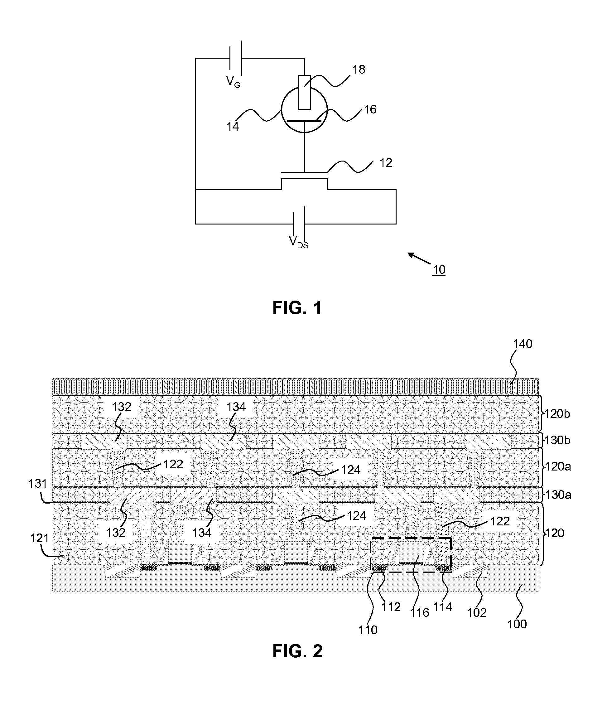
[0024]FIG. 1 schematically depicts a sensor device;

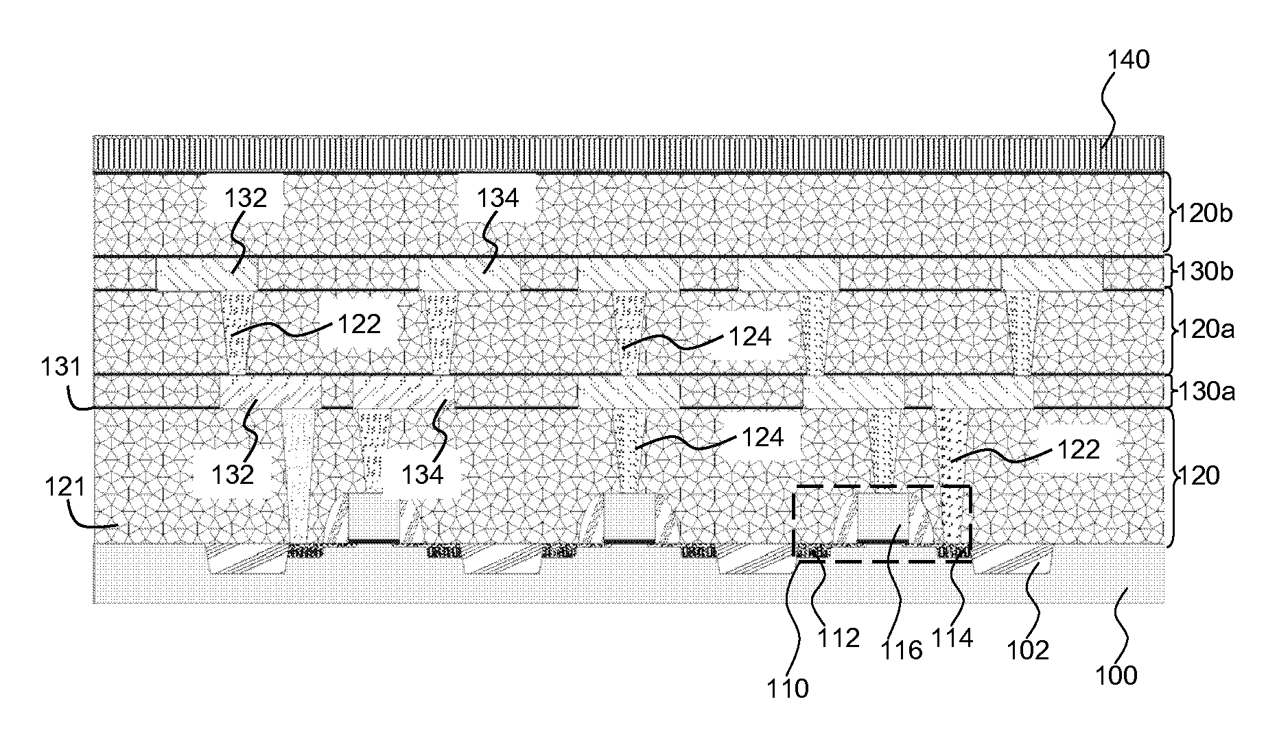
[0025]FIG. 2 schematically depicts an intermediate structure after a first step of an embodiment of the method of the present invention;

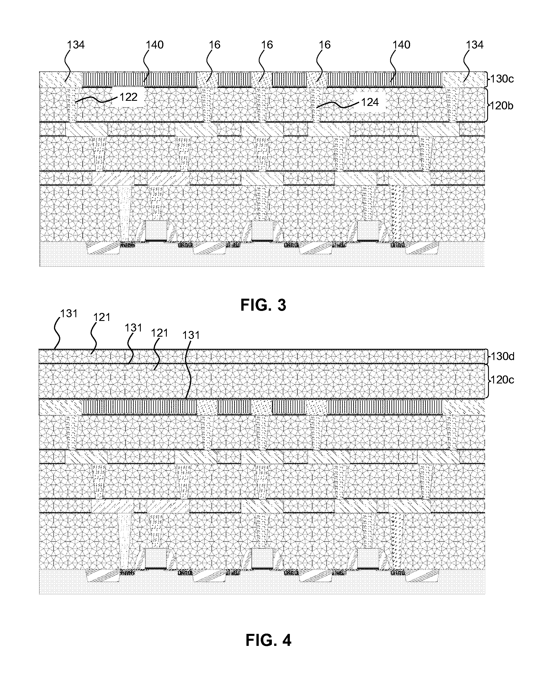
[0026]FIG. 3-7 schematically depict various intermediate structures after subsequent steps of an embodiment of the method of the present invention;

[0027]FIG. 8 schematically depicts a top view of a sensor device in accordance with an embodiment of the present invention;

[0028]FIG. 9 schematically depicts a cross section of the sensor device along the line A-A′; and

[0029]FIG. 10 schematically depicts a cross section of the sensor device along the line B-B′.

DETAILED DESCRIPTION OF THE DRAWINGS

[0030]It should be understood that the Figures are merely schematic and are not drawn to scale. It should also be understood that the same reference numerals are u...


PUM

PropertyMeasurementUnit
Timeaaaaaaaaaa
Electric potential / voltageaaaaaaaaaa
Temperatureaaaaaaaaaa

Abstract

Disclosed is a sensor device (10) comprising a substrate (100) carrying a sensing element (110), and a metallization stack on said substrate for providing interconnections to said sensing element, the metallization stack comprising a plurality of patterned metal layers (130a-d) separated by insulating layers (120a-d), wherein a first metal layer (130c) comprises an electrode portion (16) conductively connected to the sensing element, and a further metal layer (130d) facing the first metal layer comprises a reference electrode portion (18), the electrode portion and the reference electrode portion being separated by a fluid channel (14) accessible from the top of the metallization stack. A method of manufacturing such a sensor device is also disclosed.

Description

FIELD OF THE INVENTION[0001]The present invention relates to a sensor device comprising a substrate carrying a sensing element, and a metallization stack on said substrate for providing interconnections to said sensing element.[0002]The present invention further relates to a method of manufacturing such a sensor device.BACKGROUND OF THE INVENTION[0003]Due to advances in semiconductor technology, it has become feasible to detect single capture events on a sensing surface of sensors that are integrated in a monolithic circuit. An example of such a sensor is disclosed in PCT patent application WO 2009 / 047703, in which a capture molecule forms an insulating layer of a capacitor, with the plates of the capacitor formed by a conductive sensing surface and a fluid sample respectively. A capture event causes a change in the dielectric constant of the insulating layer including the volume directly above the sensor surface in which a capture event takes place, which affects the capacity of th...

Claims


Application Information

Patent Timeline
IPC IPC(8): G01N27/327H01L21/02G01N27/30
CPCG01N27/4145
Inventor BOCCARDI, GUILLAUMELAMBERT, MAGALI HUGUETTE ALICE
Owner NXP BV
Why Eureka
Try Eureka