Light emitting diode

a technology of light-emitting diodes and heat-emitting components, which is applied in the direction of basic electric elements, electrical apparatus, semiconductor devices, etc., can solve the problems of not being able to achieve high-density led placement, not being able to ensure heat-emitting performance, etc., to achieve the effect of improving both heat-emitting performance and density of led placemen

Inactive Publication Date: 2012-02-16
PANASONIC CORP
View PDF4 Cites 21 Cited by
  • Summary
  • Abstract
  • Description
  • Claims
  • Application Information

AI Technical Summary

Benefits of technology

[0007]It is an object of the present invention to provide a light emitting diode, w...

Problems solved by technology

However, it is difficult to secure a heat dissipation member to this kind of light emitting diode.
Thus, there is a problem not to be able to ensure heat dissipation performance.
Thus, there is a problem not to be able to achieve hi...

Method used


Image

  • Light emitting diode
  • Light emitting diode
  • Light emitting diode

Examples


embodiment 1

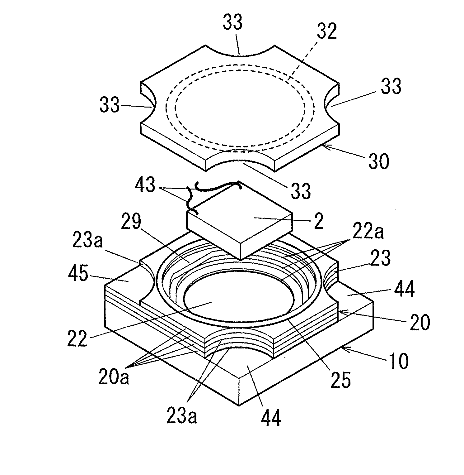
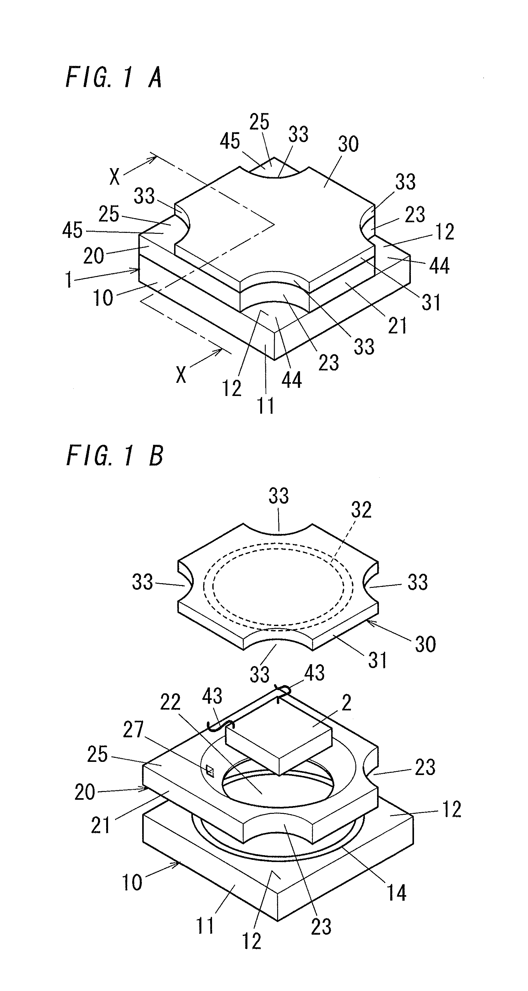
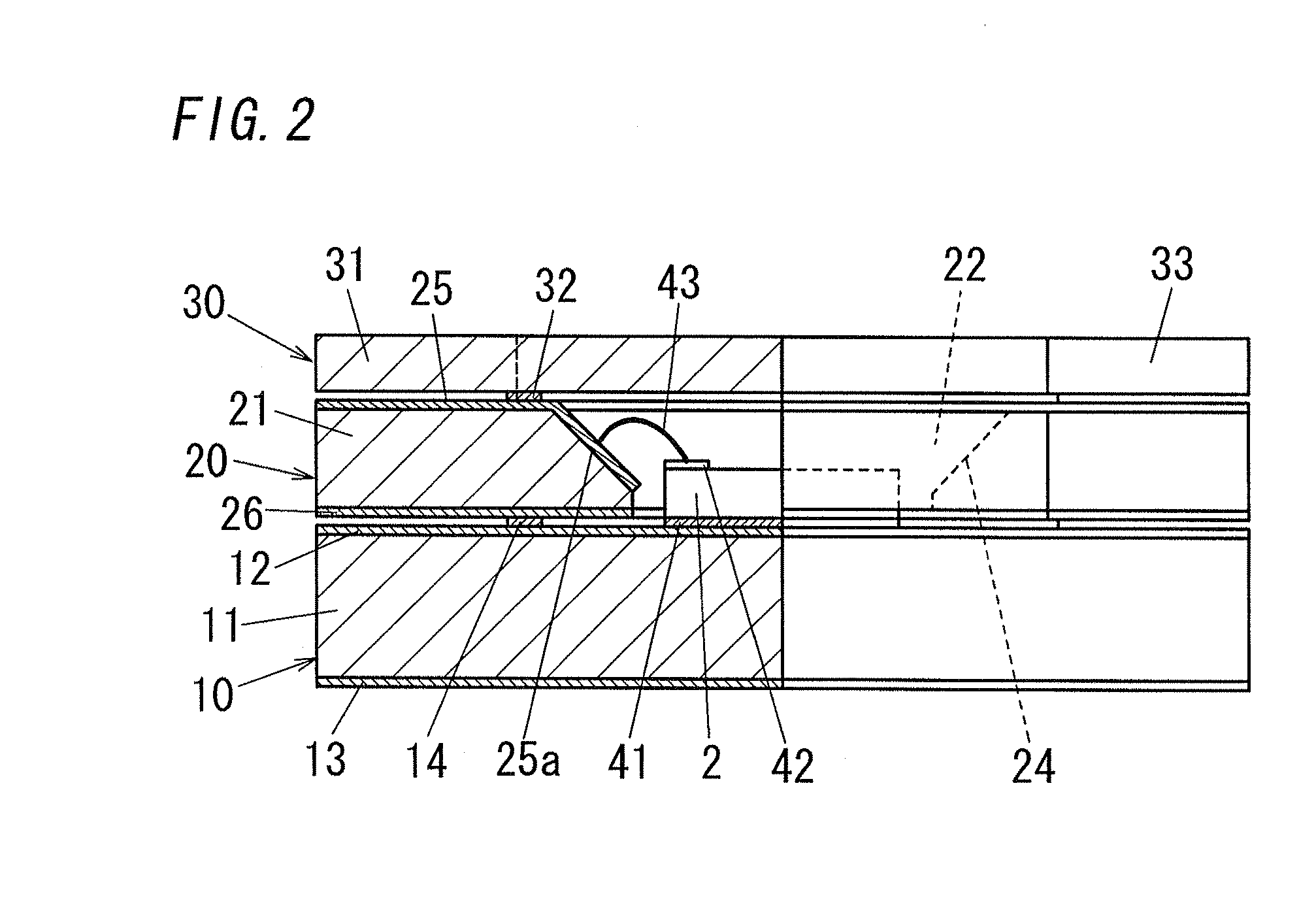
[0022]As shown in FIGS. 1A and 1B, a light emitting diode of the present embodiment comprises a light emitting diode chip (LED chip) 2 having high brightness, a package 1 in which the LED chip 2 is housed, and first and second connection electrodes 44, 45. The package 1 is a three-layered laminated body comprising a submount substrate 10, a frame body 20 and a window cover 30. The package 1 is formed into a rectangular shape (a square shape in figures) as viewed from the front (as viewed from the light irradiation direction, that is, as viewed from an upper side in FIG. 1A). The package 1 has a configuration explained below, and thereby can be formed into equal to or less than 3 mm-square as viewed from the front, and thickness thereof can be set to be about 1 mm.

[0023]The frame body 20 is provided with a storage hole 22 as a through-hole penetrated in the front and back direction. The window cover 30 is laminated on the submount substrate 10 via the frame body 20, and then the subm...

embodiment 2

[0049]As shown in FIGS. 3A and 3B, the frame body 20 of the present embodiment is formed by lamination of a plurality of sheeted frame boards 20a (four frame boards is shown in figures). Each frame board 20a is provided in its central part with a hole 22a penetrated in the front and back direction. Then, the storage hole 22 is formed by superposition of a plurality holes 22a associated with lamination of the plurality of frame boards 20a. Each frame board 20a that doesn't include one frame board 20a has the hole 22a penetrated into a circular-shape. On the other hand, said one frame board 20a has the hole 22a penetrated into generally a D-shape, like a circle cut off by a chord, as shown in FIG. 3B.

[0050]Furthermore, the plurality of holes 22a have a different diameter. A frame board 20a laminated directly on the submount substrate 10 is provided with the hole 22a having the smallest diameter, and then the remaining frame boards 20a are laminated so that diameters of the holes 22a i...


PUM


Abstract

A light emitting diode comprises a LED chip, a package in which the LED chip is housed, and a connection electrode electrically connected to an element electrode with which the LED chip is provided. The package is a laminated body comprising at least a submount substrate and a frame body, and the LED chip is fixedly-mounted on one surface of the submount substrate, and the frame body is laminated on the one surface of the submount substrate and is provided with a through-hole in which the LED chip is stored. The connection electrode is formed on at least either the one surface of the submount substrate or one surface of the frame body facing toward a light irradiation direction, while being exposed in the light irradiation direction. Therefore, the light emitting diode can improve both heat dissipation performance and density of LED placement together.

Description

TECHNICAL FIELD[0001]The invention relates generally to light emitting diodes and, more particularly, to a light emitting diode comprising a light emitting diode chip having high brightness and a package in which the light emitting diode chip is housed.BACKGROUND ART[0002]In the past, there have been proposed various light emitting diodes, comprising light emitting diode chips (LED chips) having high brightness, packages in which the LED chips are housed, and connection electrodes electrically connected to element electrodes with which the LED chips are provided. Then, most of the packages are cannon-ball type packages or surface-mount type packages. An example of the cannon-ball type packages is described in Japanese Patent Application Laid-Open No. 2006-140407 published on Jun. 1, 2006. Then, an example of the surface-mount type packages is described in Japanese Patent Application Laid-Open No. 2007-12727 published on Jan. 18, 2007.[0003]A connection electrode in a cannon-ball typ...

Claims


Application Information

Patent Timeline
IPC IPC(8): H01L33/62
CPCH01L33/486H01L33/58H01L33/62H01L33/647H01L2224/48091H01L2224/84385H01L2924/00014H01L2224/45124H01L2224/45144H01L2924/00
Inventor URANO, YOUJI
Owner PANASONIC CORP
Why Eureka
Try Eureka