Method of manufacturing microlens array, method of manufacturing solid-state image sensor, and solid-state image sensor
a manufacturing method and microlens array technology, applied in the field of manufacturing microlens arrays, can solve the problems of alignment errors between microlenses of different colors, the number of manufacturing processes increases, etc., and achieve the effect of simplifying the manufacturing process of microlense arrays and preventing alignment errors
- Summary
- Abstract
- Description
- Claims
- Application Information
AI Technical Summary
Benefits of technology
Problems solved by technology
Method used
Image
Examples
first embodiment
[0029]In the present invention, a latent pattern for forming red, green, and blue microlenses in one exposure process by using a photomask in which lens patterns for forming the red, green, and blue microlenses are arranged is formed. The latent pattern is developed to form a resist pattern. The resist pattern is then annealed to smoothen its surface, thereby forming the curved surface of the microlens.
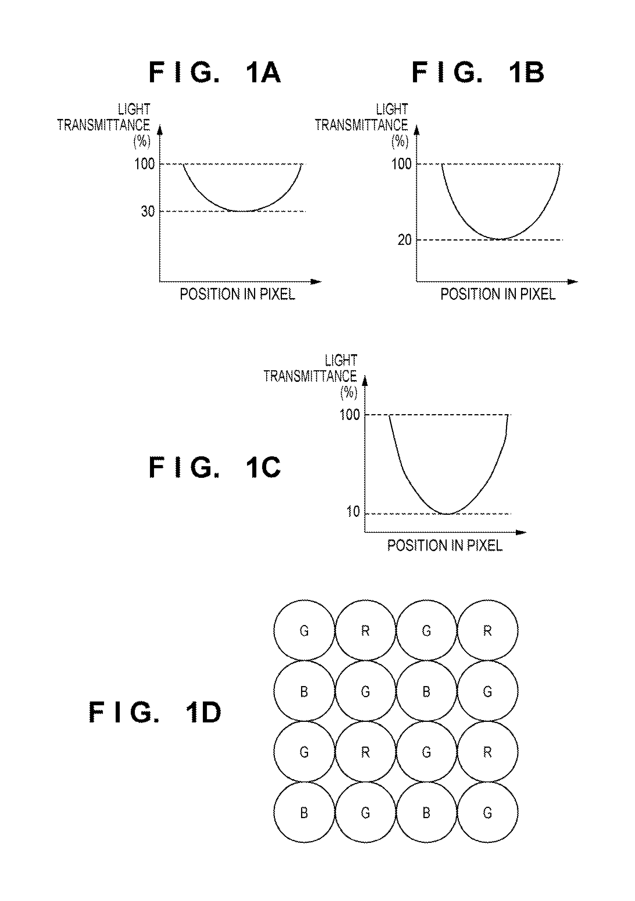
[0030]FIG. 1D is a plan view illustrating part of a photomask PM used in the first embodiment of the present invention. Reference symbols B, G, and R denote lens patterns for forming the blue, green, and red pixel microlenses, respectively. FIGS. 1A, 1B and 1C exemplify the exposure light transmittances of the lens patterns for forming the blue, green, and red pixel microlenses. The exposure light transmittance distribution can be given by the area intensity method. The area intensity method is a method of determining intensities in accordance with dot pattern densities. The dot patte...
sixth embodiment
[0055]The sixth embodiment uses the photomask having different exposure light transmittance distributions between the lens pattern for forming the microlens 9-E for the AF pixel FP and the lens pattern for forming the microlens 9-D for the normal pixel NP. Assume that the microlens 9-E for the AF pixel FP and the microlens 9-D for the normal pixel NP have different heights and different curvatures. Assume also that the microlenses 9-E are spaced apart from each other by one or more pixels via the microlenses 9-D. That is, at least one of the microlenses 9-D is arranged between one of the microlenses 9-E and another of the microlenses 9-E.
[0056]When a microlens is larger than a circle inscribed in a pixel region indicated by a dotted line, as shown in FIG. 12C, continuity of the photomask transmittance is lost at a boundary where the microlenses are adjacent to each other, as shown in FIG. 12A or 12B. A microlens 9-D-1 for the normal pixel NP adjacent to the microlens 9-E for the AF ...
PUM
| Property | Measurement | Unit |
|---|---|---|
| thickness | aaaaa | aaaaa |
| transmittance | aaaaa | aaaaa |
| width | aaaaa | aaaaa |
Abstract
Description
Claims
Application Information


