Autotuned screen printing process

a screen printing and autotuned technology, applied in the direction of sustainable manufacturing/processing, semiconductor/solid-state device testing/measurement, instruments, etc., can solve the problems of low cost of forming high-quality solar cells, poor device performance, and device yield issues

Active Publication Date: 2012-02-23
APPLIED MATERIALS INC
View PDF3 Cites 17 Cited by
  • Summary
  • Abstract
  • Description
  • Claims
  • Application Information

AI Technical Summary

Problems solved by technology

The high market growth rate in combination with the need to substantially reduce solar electricity costs has resulted in a number of serious challenges for inexpensively forming high quality solar cells.
The mis-alignment of a screen printing pattern on a substrate surface due to errors in the positioning of a substrate on the automated transferring devices, or defects on the edge of the substrate, can lead to poor device performance, and thus device yield issues.
Manual calibration of the positioning of the substrate within the system can be time consuming and require frequent adjustment based on differences in batches of substrates or drift in the calibrated position of the substrate.

Method used


Image

  • Autotuned screen printing process
  • Autotuned screen printing process
  • Autotuned screen printing process

Examples


Embodiment Construction

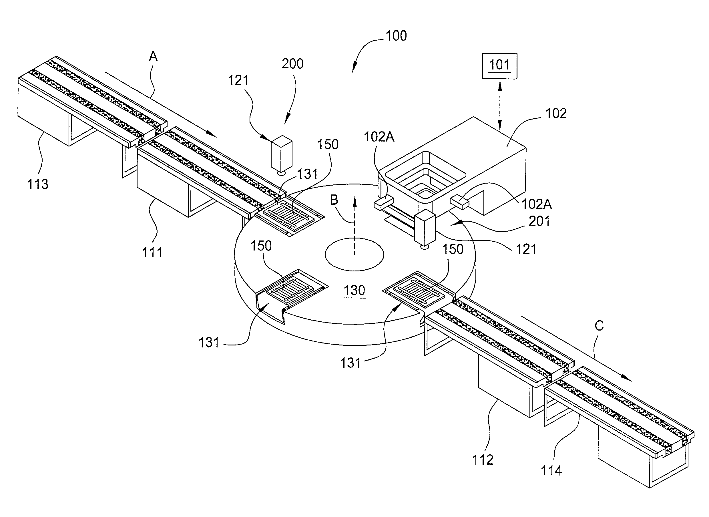
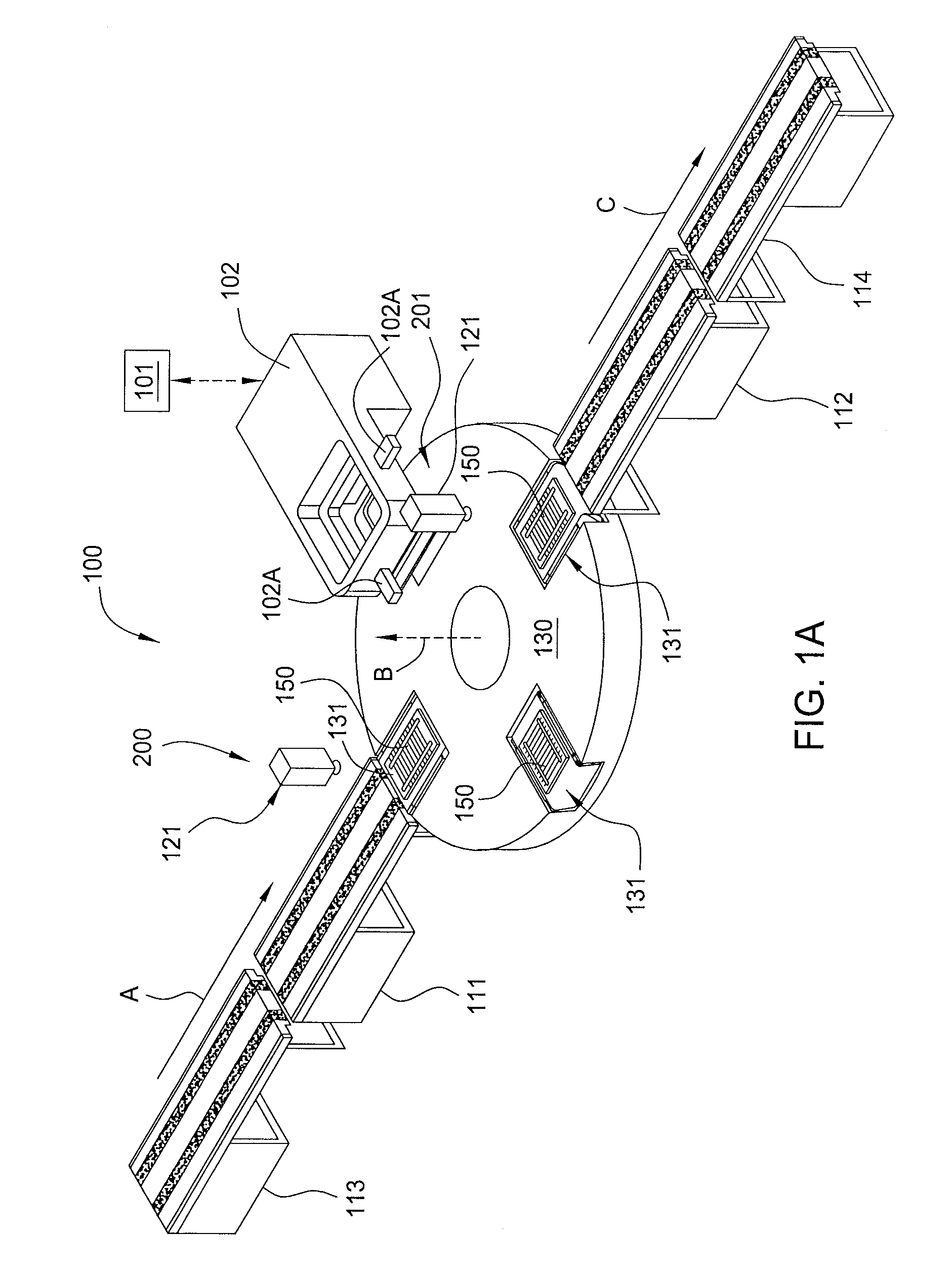
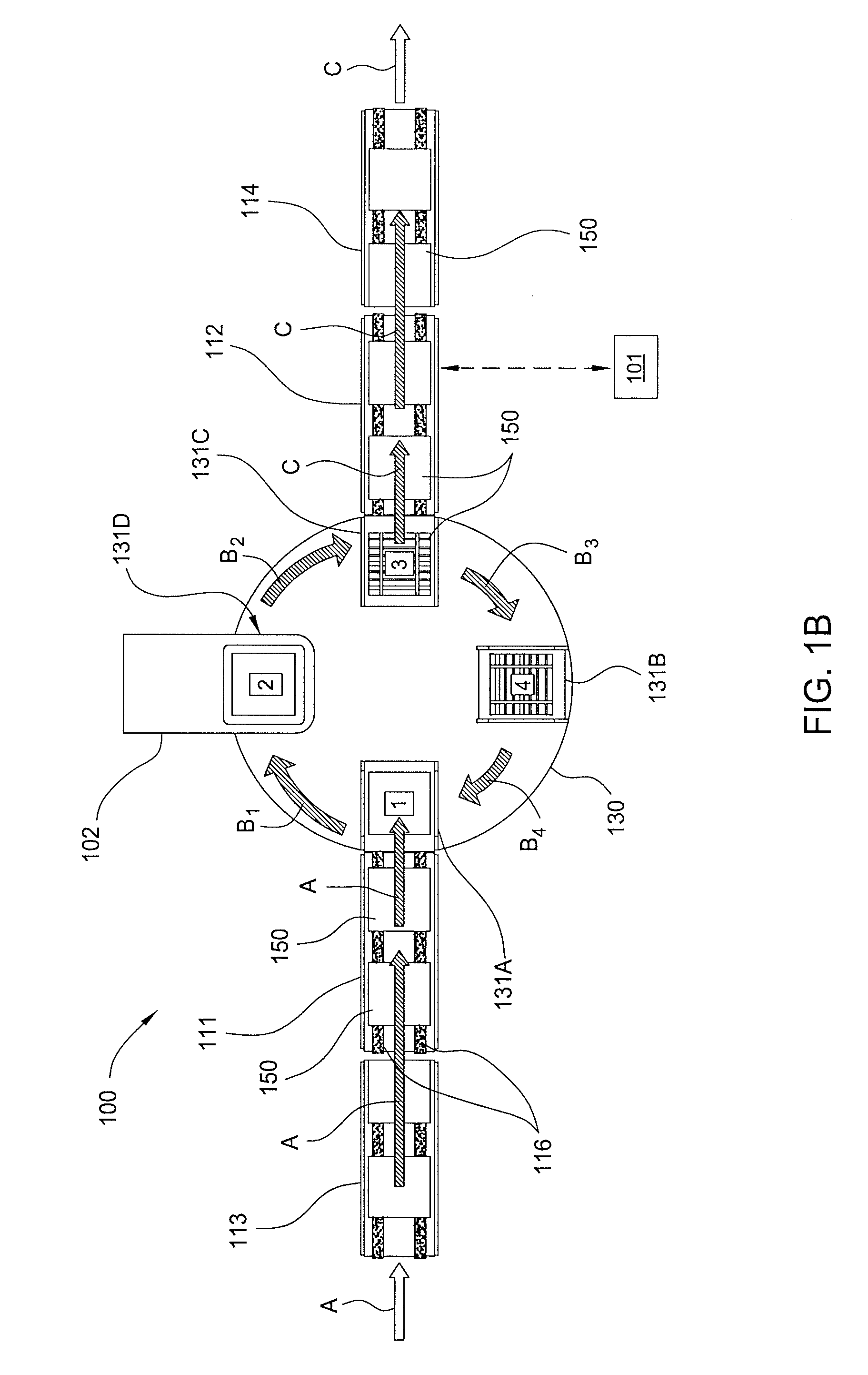
[0025]Embodiments of the present invention provide an apparatus and method for processing substrates in a screen printing system that utilizes an improved substrate transferring, aligning, and screen printing process that can improve the device yield performance and cost-of-ownership (CoO) of a substrate processing line. In one embodiment, the screen printing system, hereafter system, is adapted to perform a screen printing process within a portion of a crystalline silicon solar cell production line in which a substrate is patterned with a desired material in two or more layers and is then processed in one or more subsequent processing chambers. The subsequent processing chambers may be adapted to perform one or more bake steps and one or more cleaning steps. In one embodiment, the system is a module positioned within the Softline™ tool available from Baccini S.p.A., which is owned by Applied Materials, Inc. of Santa Clara, Calif. While the discussion below primarily discusses the p...


PUM


Abstract

Embodiments of the invention generally provide apparatus and methods of screen printing a pattern on a substrate. In one embodiment, a patterned layer is printed onto a surface of a substrate along with a plurality of alignment marks. The locations of the alignment marks are measured with respect to a feature of the substrate to determine the actual location of the patterned layer. The actual location is compared with the expected location to determine the positional error of the patterned layer placement on the substrate. This information is used to adjust the placement of a patterned layer onto subsequently processed substrates.

Description

BACKGROUND OF THE INVENTION[0001]1. Field of the Invention[0002]Embodiments of the present invention generally relate to a system and process for screen printing a multiple layer pattern on a surface of a substrate.[0003]2. Description of the Related Art[0004]Solar cells are photovoltaic (PV) devices that convert sunlight directly into electrical power. Solar cells typically have one or more p-n junctions. Each p-n junction comprises two different regions within a semiconductor material where one side is denoted as the p-type region and the other as the n-type region. When the p-n junction of a solar cell is exposed to sunlight (consisting of energy from photons), the sunlight is directly converted to electricity through the PV effect. Solar cells generate a specific amount of electric power and are tiled into modules sized to deliver the desired amount of system power. Solar modules are joined into panels with specific frames and connectors. Solar cells are commonly formed on silic...

Claims


Application Information

Patent Timeline
Patent Type & Authority Applications(United States)
IPC IPC(8): H01L21/66B05C11/00
CPCB41F15/0818Y02E10/50B41P2215/10B41P2215/114B41P2233/52H01L21/67259H01L31/022425H01L31/18H01L31/1876H05K3/0097H05K3/1216H05K2201/09781H05K2201/09918H05K2203/163B41F15/20Y02P70/50B41F15/08H01L31/04
Inventor BACCINI, ANDREAGALIAZZO, MARCO
Owner APPLIED MATERIALS INC
Why Eureka
Try Eureka