Detector System for Use with Transmission Electron Microscope Spectroscopy

a technology of transmission electron microscope and detector system, which is applied in the direction of material analysis using wave/particle radiation, instruments, nuclear engineering, etc., can solve the problem of reducing the resolution of the detector, and achieve the effect of improving the performance of the transmission electron microscop

Active Publication Date: 2012-03-01
FEI CO
View PDF13 Cites 25 Cited by
  • Summary
  • Abstract
  • Description
  • Claims
  • Application Information

AI Technical Summary

Benefits of technology

[0014]An object of the invention is to improve the performance of transmission electron microscopes.

Problems solved by technology

TEMs commonly use charged-couple device (“CCD”) detectors, which are damaged by high energy electrons.
The intervening scintillator reduces resolution of the detector.

Method used


Image

  • Detector System for Use with Transmission Electron Microscope Spectroscopy
  • Detector System for Use with Transmission Electron Microscope Spectroscopy
  • Detector System for Use with Transmission Electron Microscope Spectroscopy

Examples


Embodiment Construction

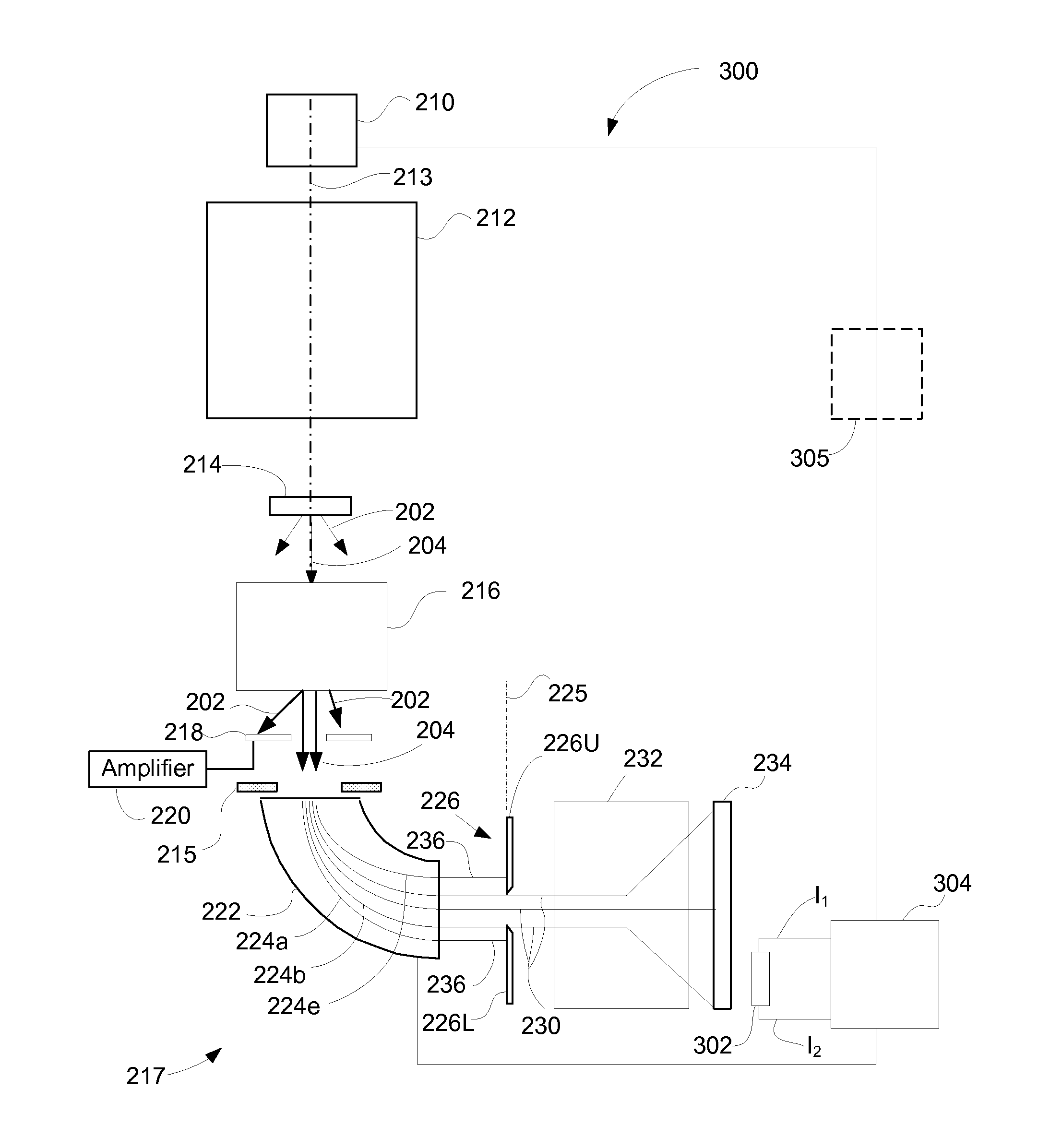
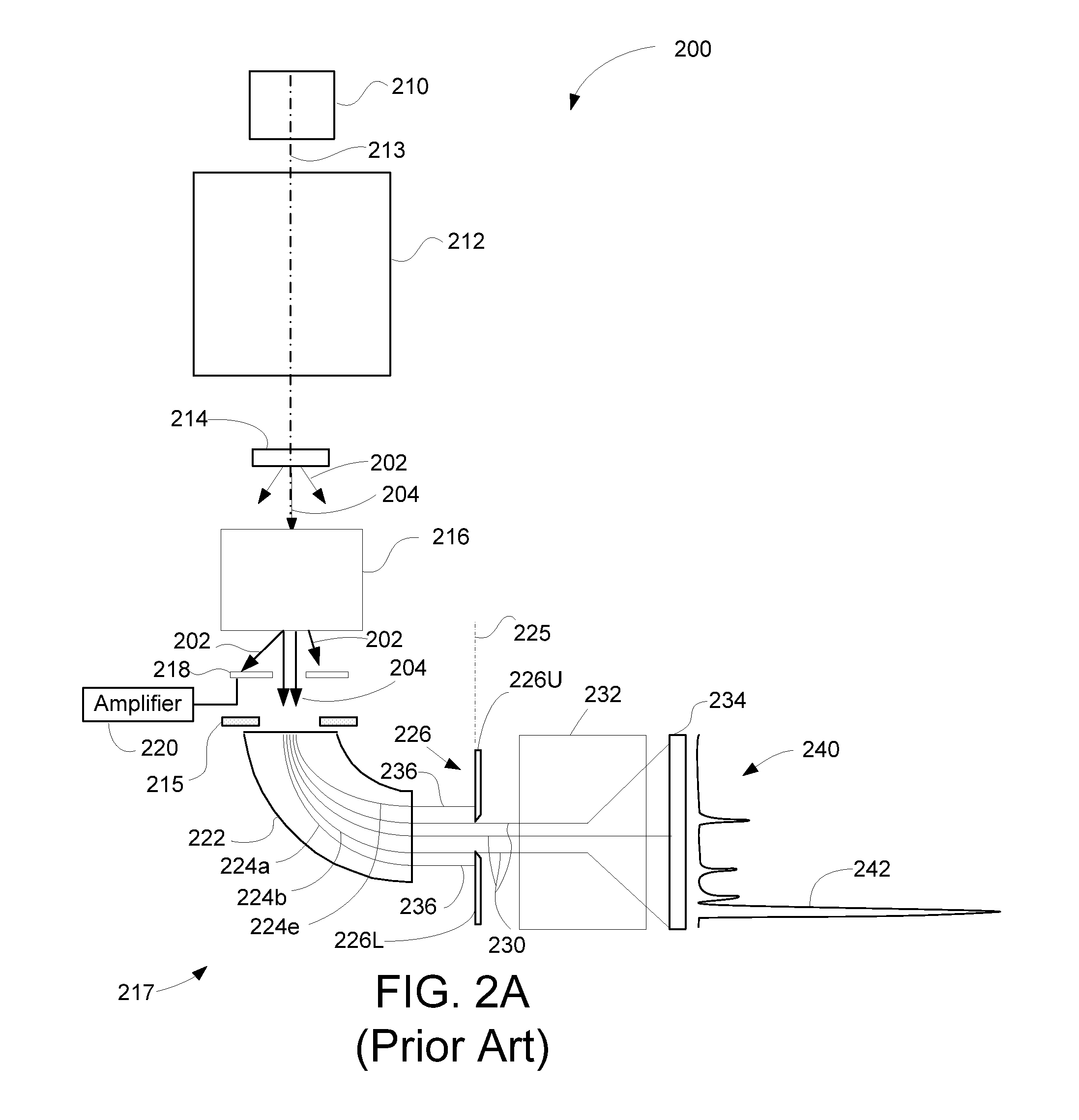
[0024]In transmission electron microscopy, electrons that pass through the sample carry information about the sample and produce a pattern on a primary camera detector. The pattern may correspond to, for example, an image of the sample, a diffraction pattern, or an energy loss spectrum. The position of the pattern on the detector is subject to constant small shifts, from a variety of causes. Temperature changes and mechanical vibration may cause small changes in the position of components in the electron beam column, which can shift the electron pattern on the detector. Also, electrical instabilities in the primary electron column can cause the energy of electrons in the primary beam to vary, which changes the electron position in the detector. When electrons are measured in a spectrometer for EELS, electrical and mechanical drift in the spectrometer can also contribute to changes in the spectrum position. The instability in position of the spectrum affects the resolution of the mic...


PUM

PropertyMeasurementUnit
thicknessaaaaaaaaaa
energy lossaaaaaaaaaa
thickaaaaaaaaaa

Abstract

A detector system for a transmission electron microscope includes a first detector for recording a pattern and a second detector for recording a position of a feature of the pattern. The second detector is preferably a position sensitive detector that provides accurate, rapid position information that can be used as feedback to stabilize the position of the pattern on the first detector. In one embodiment, the first detector detects an electron energy loss electron spectrum, and the second detector, positioned behind the first detector and detecting electrons that pass through the first detector, detects the position of the zero-loss peak and adjusts the electron path to stabilize the position of the spectrum on the first detector.

Description

[0001]This application claims priority from U.S. Provisional Patent Application 61 / 376,973, filed Aug. 25, 2010, which is hereby incorporated by reference.TECHNICAL FIELD OF THE INVENTION[0002]The present invention relates to detectors for transmission electron microscopes.BACKGROUND OF THE INVENTION[0003]In a transmission electron microscope, a beam of high-energy electrons is directed toward a thin sample. Electrons in the beam interact with the sample as they pass through it and are collected below the sample. Some electrons pass through the sample relatively unhindered; others are deflected, absorbed, or lose energy. The electrons that pass through the sample carry information about the sample and produce a pattern on a detector. The pattern may correspond to, for example, an image of the sample, a diffraction pattern, or a spectrum of electron energy. Different imaging and analysis techniques use different characteristics of the transmitted electrons to form an image or to dete...

Claims


Application Information

Patent Timeline
Patent Type & Authority Applications(United States)
IPC IPC(8): H01J47/00G01N23/00
CPCH01J37/05H01J37/244H01J37/26H01J2237/05H01J2237/2817H01J2237/2446H01J2237/24485H01J2237/2802H01J2237/24455
Inventor LUECKEN, UWEKOOIJMAN, CORNELIS SANDERSCHUURMANS, FRANK JEROEN PIETER
Owner FEI CO
Why Eureka
Try Eureka