Light emitting unit array and projection system

a technology of light emitting units and arrays, applied in the field of light emitting unit arrays and display devices, can solve the problems of reducing the volume of products, difficult to achieve high projection brightness of such products, and further have small volume,

Active Publication Date: 2012-03-01
IND TECH RES INST
View PDF19 Cites 65 Cited by
  • Summary
  • Abstract
  • Description
  • Claims
  • Application Information

AI Technical Summary

Benefits of technology

[0014]In order to make the aforementioned and other objects, features and advantages of the disc...

Problems solved by technology

For burying the projection system in the portable electronic products, a problem needs to be overcome is the reduction of the volume of the product.
Accordingly, it is difficult for such products to achieve high projection brightness and further have small volume, e.g. a projection system with mic...

Method used


Image

  • Light emitting unit array and projection system
  • Light emitting unit array and projection system
  • Light emitting unit array and projection system

Examples


first embodiment

[0030]FIGS. 4a through 4i depict a fabricating method of a light emitting unit array according to the disclosure. Referring to FIG. 4a, a doped semiconductor material thin layer 222a and a plurality of light collimation structures 224 are formed on a substrate 220. In the embodiment, the substrate 220 is, for example, a sapphire substrate or other suitable substrate facilitating applying in the epitaxy process. The light collimation structures 224 are arranged in an array on the doped semiconductor material thin layer 222a and two adjacent light collimation structures 224 are separated by a gap G. The light collimation structures 224 are formed on the doped semiconductor material thin layer 222a by an optical coating process, for example.

[0031]In the present embodiment, the light collimation structures 224 can be distributed Bragg reflectors (BDRs). Namely, the light collimation structures 224 are the multi-layers formed by material layers with different refractive index, such as Ta...

third embodiment

[0049]FIGS. 9a through 9g depict a fabricating method of a light emitting unit array according to the disclosure. Referring to FIG. 9a, the first type doped semiconductor layer 522, the active layer 524, and the second type doped semiconductor layer 526 are sequentially formed on the substrate 510. The substrate 510 is, for example, a sapphire substrate or other suitable substrate facilitating applying in the epitaxy process. The first type doped semiconductor layer 522 can be an n-type doped semiconductor layer and the second type doped semiconductor layer 526 can be a p-type doped semiconductor layer. The n type doped semiconductor material and the p type doped semiconductor material selected in the present embodiment can, for example, be an n type doped GaN and a p type doped GaN. Nevertheless, in one embodiment, the n type doped semiconductor material and the p type doped semiconductor material can be other semiconductor materials doped with required dopant such as GaAlN, GaInN,...

fourth embodiment

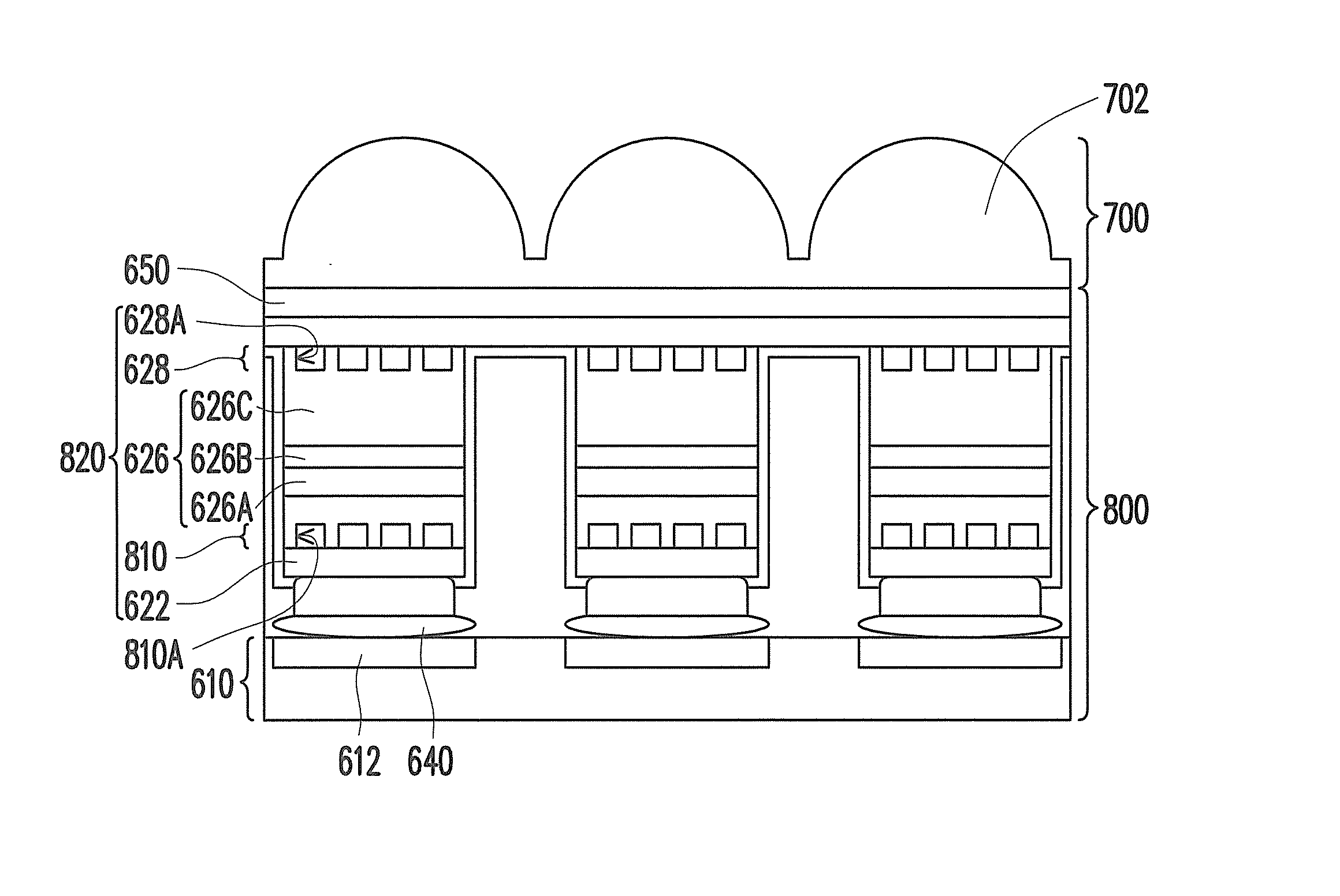
[0056]FIG. 10 schematically illustrates a light emitting unit array and a μ-lens array according to the disclosure. Referring to FIG. 10, in the present embodiment, the μ-lens array 700 is disposed on the light emitting unit array 600 and has a plurality of μ-lens 702. The light emitting unit array 600 includes a plurality of μ-LEDs 620 arranged in an array on the substrate 610 and each μ-LED 620 is configured with the electrode 640 and the transparent conductive layer 650 at the two opposite sides thereof so as to electrically connected to an external circuit. Each electrode 640 is, for example, bonded to the circuit element 612 on the substrate 610 through the corresponding pad 660.

[0057]In the present embodiment, each of the μ-LEDs 620 includes a reflection layer 622, a contact layer 624, a light emitting structure 626, and a light collimation structure 628. The light emitting structure 626 includes the first type doped semiconductor layer 626A, the active layer 525B, and the sec...


PUM


Abstract

A light emitting unit array including a plurality of micro-light emitting diodes (μ-LEDs) is provided. The micro-light emitting diodes are arranged in an array on a substrate, and each of the micro-light emitting diodes includes a reflection layer, a light emitting structure, and a light collimation structure. The light emitting structure is disposed on the reflection layer, and includes a first type doped semiconductor layer, an active layer, and a second type doped semiconductor layer that are stacked sequentially. At least a portion of the first type doped semiconductor layer, the active layer, and the second type doped semiconductor layer are sandwiched between the reflection layer and the light collimation structure.

Description

CROSS-REFERENCE TO RELATED APPLICATION[0001]This application claims the priority benefits of U.S. provisional application Ser. No. 61 / 377,462, filed on Aug. 27, 2010 and Taiwan application serial no. 100129591, filed on Aug. 18, 2011. The entirety of each of the above-mentioned patent applications is hereby incorporated by reference herein and made a part of this specification.BACKGROUND OF THE DISCLOSURE[0002]1. Field of the Disclosure[0003]The disclosure relates to a light emitting unit array and display device, and particularly, to a micro-light emitting diode array (μ-LED array) and a projection system using the μ-LED array as the projection imaging source.[0004]2. Description of Related Art[0005]LED has the characteristics of high efficiency, long lifespan, etc. and thus the LED light source has been widely applied. The application of the LED in the micro-projection system facilitates a dramatic revolution of the projection and display products. The micro-projection system can ...

Claims


Application Information

Patent Timeline
IPC IPC(8): G03B21/28H01L33/10H01L33/08
CPCG03B21/2033H01L27/156H01L33/46H01L33/405H01L33/0079H01L33/0093
Inventor HUANG, CHEN-YANGCHAO, CHIA-HSINYEH, WEN-YUNG
Owner IND TECH RES INST
Why Eureka
Try Eureka