FLIP-CHIP ASSEMBLY COMPRISING AN ARRAY OF VERTICAL CAVITY SURFACE EMITTING LASERS (VCSELSs)

a technology of lasers and flip-chips, which is applied in the field of flip-chip assemblies comprising an array of vertical cavity surface emitting lasers (vcsels), can solve the problems of increasing the overall cost of the semiconductor device, low manufacturing yield, and relatively low manufacturing yield of this type of semiconductor device, and achieve the effect of preventing contamination ingress

Active Publication Date: 2012-03-01
AVAGO TECH INT SALES PTE LTD
View PDF6 Cites 37 Cited by
  • Summary
  • Abstract
  • Description
  • Claims
  • Application Information

AI Technical Summary

Benefits of technology

[0009]In accordance with another illustrative embodiment, the VCSEL flip chip assembly comprises a substrate, a plurality of electrically conductive contact pads disposed on an upper surface of the substrate, a plurality of VCSEL flip chips mounted on the upper surface of the substrate, and a pattern of electrically nonconductive sealing compound disposed on the upper surface of the substrate beneath an outer periphery of each respective VCSEL flip chip. The substrate is transparent to a particular wavelength of light produced by the VCSELs. The plurality of electrically conductive contact pads disposed on the upper surface of the substrate are located in flip chip mounting areas of the upper surface of the substrate. Each VCSEL flip chip is mounted in one of the respective flip chip mounting areas of the upper surface of the substrate. Each VCSEL flip chip includes a plurality of electrically conductive contact pads that are electrically coupled via electrically conductive epoxy with respective electrically conductive contact pads disposed in the respective flip chip mounting areas of the upper surface of the substrate. Each VCSEL flip chip has at least one VCSEL that produces light of the particular wavelength and a respective aperture through which the light produced by the respective VCSEL passes out of the respective VCSEL flip chip. The VCSEL flip chips are mounted with the apertures facing the upper surface of the substrate such that most if not all of the light passing out of the apertures enters the substrate. The pattern of electrically nonconductive sealing compound disposed on the upper surface of the substrate beneath the outer peripheries of the respective VCSEL flip chips prevents ingression of contaminants into the respective optical pathways.

Problems solved by technology

However, the manufacturing yield for this type of semiconductor device is relatively low due to the fact that the semiconductor device is deemed defective and is discarded if even one of the VCSELs of the array is found to be defective.
The relatively low manufacturing yield of this type of semiconductor device increases the overall costs of the semiconductor devices.
This approach presents other difficulties, however, one of which is the difficulty associated with precisely aligning the VCSELs with their respective optical coupling elements.
Consequently, to date, using multiple semiconductor devices having only either a singlet VCSEL or a very small number of VCSELs on them to create a larger array of VCSELs is not a viable solution.

Method used


Image

  • FLIP-CHIP ASSEMBLY COMPRISING AN ARRAY OF VERTICAL CAVITY SURFACE EMITTING LASERS (VCSELSs)
  • FLIP-CHIP ASSEMBLY COMPRISING AN ARRAY OF VERTICAL CAVITY SURFACE EMITTING LASERS (VCSELSs)
  • FLIP-CHIP ASSEMBLY COMPRISING AN ARRAY OF VERTICAL CAVITY SURFACE EMITTING LASERS (VCSELSs)

Examples


Embodiment Construction

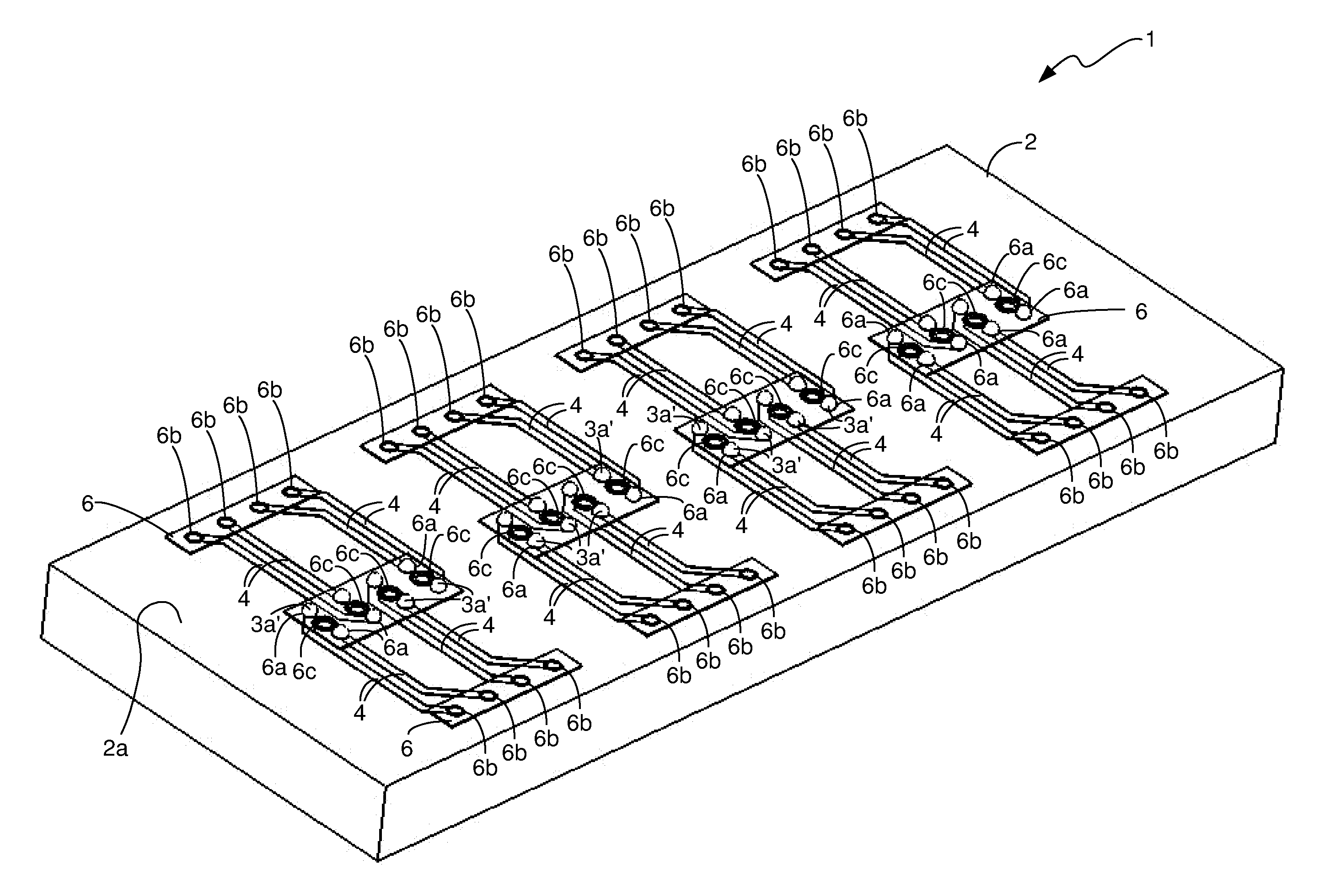
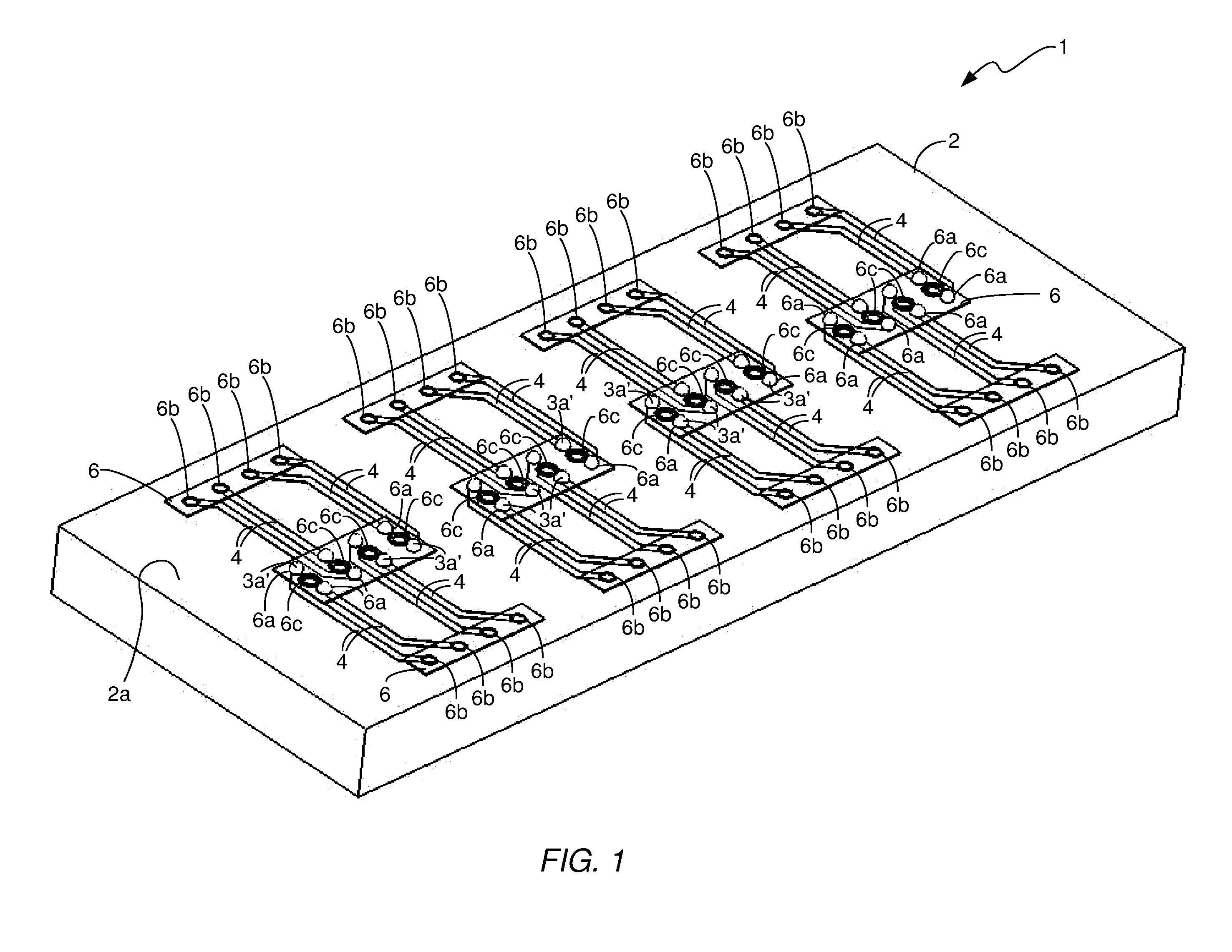
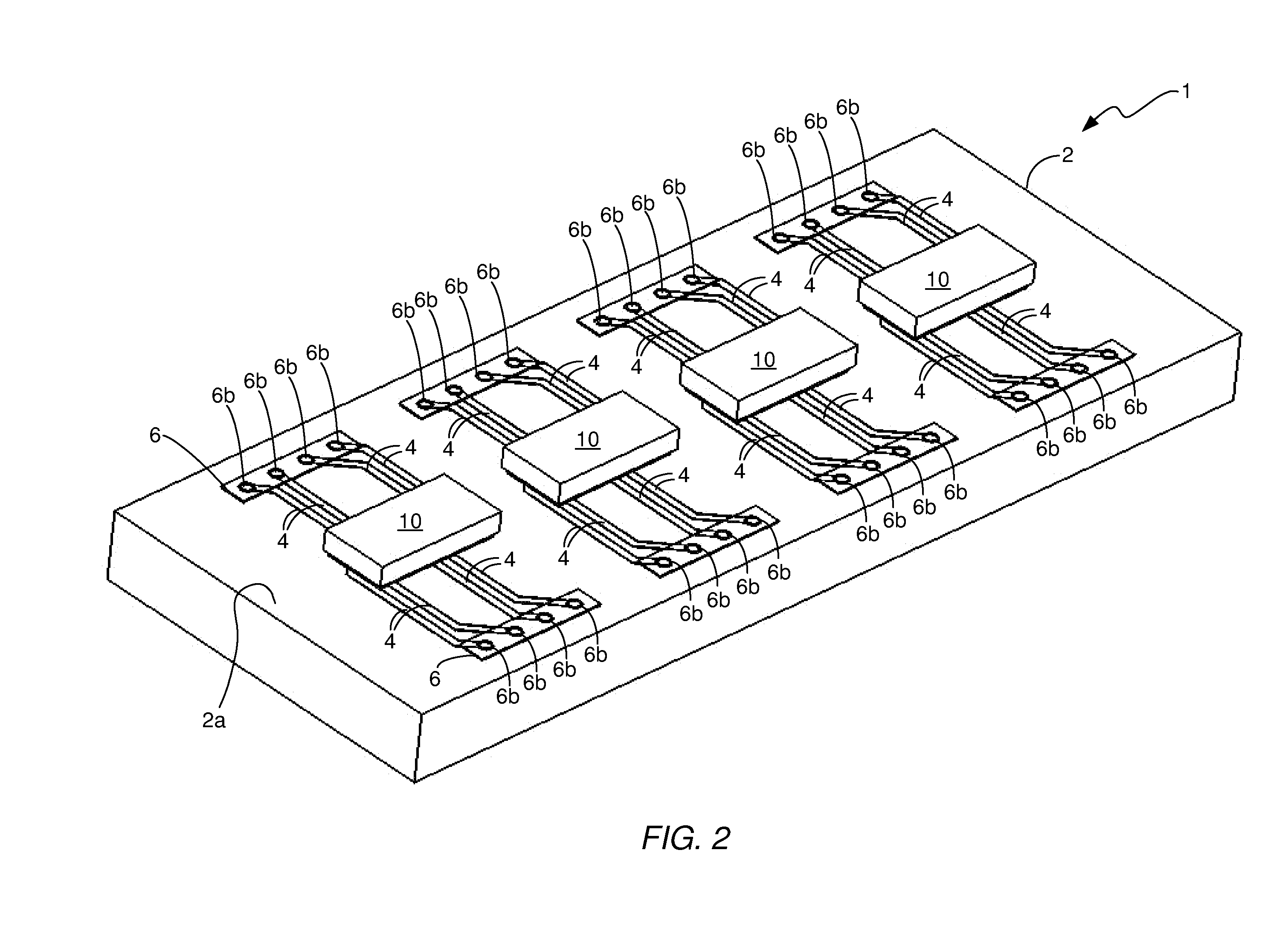
[0020]The invention takes advantage of the fact that known flip-chip assembly manufacturing technology makes it possible to manufacture flip-chip assemblies with high precision, high manufacturing yield, and high throughput. The known flip-chip assembly manufacturing process is augmented by process steps of the invention to create a VCSEL flip-chip assembly comprising a plurality of semiconductor devices having one or more VCSELs thereon, which are mounted on a substrate to form a large array of VCSELs that are precisely optically aligned with their respective optical coupling elements. This feature prevents the aforementioned problems associated with manufacturing a semiconductor device having a large number of VCSELs thereon, or creating an array of VCSELs by assembling a plurality of semiconductor devices that have either a singlet VCSEL or a small number of VCSELs thereon. Consequently, the VCSEL flip-chip assemblies can be manufactured with high precision, high manufacturing yi...


PUM


Abstract

A known flip-chip assembly manufacturing process is augmented by process steps of the invention to create a VCSEL flip-chip assembly comprising a plurality of semiconductor devices having respective arrays of a small number of VCSELs thereon, which are mounted on a substrate to form a large array of VCSELs that are precisely optically aligned with their respective optical coupling elements.

Description

TECHNICAL FIELD OF THE INVENTION[0001]The invention relates to semiconductor lasers, and more particularly, to a flip-chip assembly comprising an array of vertical cavity surface emitting lasers (VCSELs).BACKGROUND OF THE INVENTION[0002]In optical communications networks, optical transceiver and transmitter modules are used to transmit optical signals over optical fibers. The optical transceiver or transmitter module includes a laser that generates amplitude modulated optical signals that represent data, which are then transmitted over an optical fiber coupled to the transceiver or transmitter module. Various types of semiconductor lasers are typically used for this purpose, including, for example, VCSELs and edge emitting lasers, which may be further divided into subtypes that include Fabry Perot (FP) and Distributed Feedback (DFB) lasers.[0003]Some optical transmitter or transceiver modules have only a single transmit channel comprising a single laser, which is sometimes referred ...

Claims


Application Information

Patent Timeline
Patent Type & Authority Applications(United States)
IPC IPC(8): G02B6/12H01S5/42
CPCH01S5/0224H01S5/02252H01S5/423H01S5/02276H01S5/02284H01S5/02272H01L2224/73204H01L2224/97H01S5/02251H01S5/02326H01S5/0234H01S5/02345H01S5/0237
Inventor SU, CHUNG-YIWANG, TAK K.
Owner AVAGO TECH INT SALES PTE LTD
Why Eureka
Try Eureka