Semiconductor device integrated with converter and package structure thereof

a technology of semiconductor devices and converters, applied in semiconductor devices, semiconductor/solid-state device details, electrical apparatuses, etc., can solve problems such as power loss during voltage conversion, and achieve the effect of reducing the turn-on resistance and reducing the power loss during power supply conversion

Active Publication Date: 2012-03-08
SINOPOWER SEMICON
View PDF3 Cites 5 Cited by
  • Summary
  • Abstract
  • Description
  • Claims
  • Application Information

AI Technical Summary

Benefits of technology

[0014]In conclusion, the semiconductor device of the present invention includes the high-side transistor device and the low-side transistor device on the same semiconductor substrate, so that only a chip holder is required to dispose the semiconductor device in the package structure, and the area of the semiconductor substrate or the sizes of the high-side transistor device and the low-side transistor device in the semiconductor device disposed on the chip holder can be increased to reduce the turn-on resistance between the drain and the source of the high-side transistor device and the turn-on resistance between the drain and the source of the low-side transistor device. Thus, the power loss during power supply conversion can be reduced.

Problems solved by technology

Therefore, the resistance between the source 14b of the high-side NMOSFET device 14 and the drain of the low-side NMOSFET device 16 is restricted by the transmission path and the resistance may further cause the power loss during voltage conversion.

Method used


Image

  • Semiconductor device integrated with converter and package structure thereof
  • Semiconductor device integrated with converter and package structure thereof
  • Semiconductor device integrated with converter and package structure thereof

Examples


first embodiment

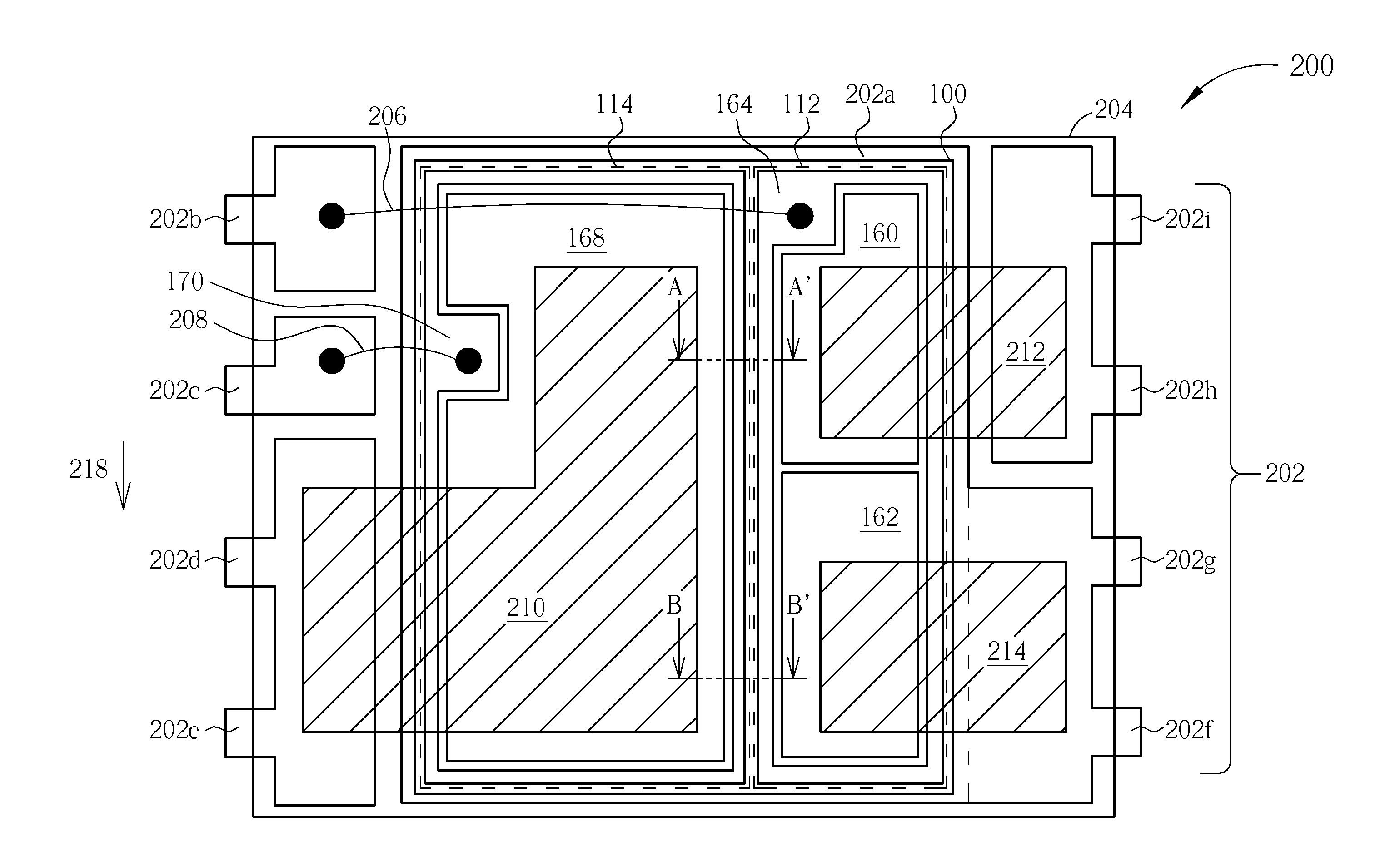
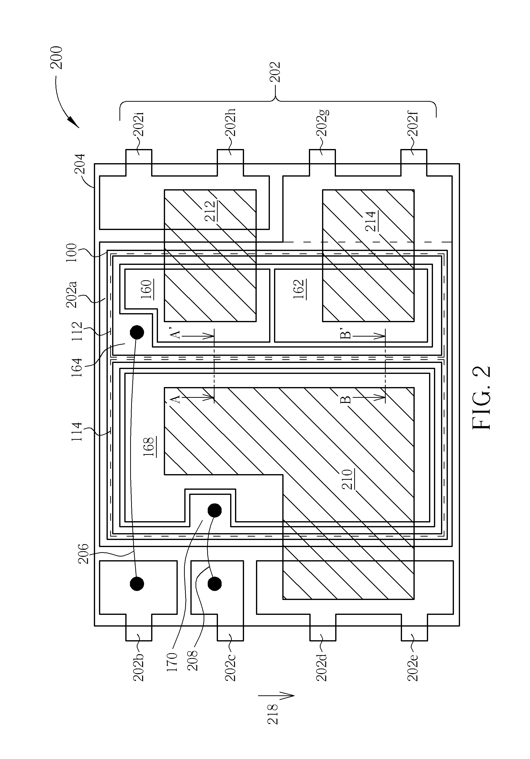
[0042]In addition, the N-type doped high-side source region of the present invention is not limited to be electrically connected to the N-type semiconductor substrate by means of the high-side source metal layer and the first contact plug. Please refer to FIG. 11. FIG. 11 is a cross-sectional view of a semiconductor device according to a second exemplary embodiment of the present invention. Same components are denoted by same numerals as the first exemplary embodiment in the following exemplary embodiments, and same structures are not redundantly detailed. As shown in FIG. 11, compared to the first exemplary embodiment, the semiconductor device 300 of this exemplary embodiment excludes the high-side source metal layer 162 and the first contact plug 136 used for electrically connecting the doped high-side source region 126 to the semiconductor substrate 102, and a second interlayer dielectric layer 302 of this exemplary embodiment totally covers a second contact plug 304 for electric...

first exemplary embodiment

[0044]In addition, the structure of the lead frame is not limited to the structures of the previous exemplary embodiments. Please refer to FIG. 13. FIG. 13 is a top-view illustrating a package structure of a semiconductor device according to a third exemplary embodiment of the present invention. As shown in FIG. 13, compared to the first exemplary embodiment, the fifth lead 202f, the sixth lead 202g, the seventh lead 202h, and the eighth lead 202i in the package structure 450 of the semiconductor device 400 according to this exemplary embodiment are arranged along a direction reverse to the direction of the That is to say, the fifth lead 202f, the sixth lead 202g, the seventh lead 202h, and the eighth lead 202i are arranged along the first direction 218 in sequence, and the fifth lead 202f, the sixth lead 202g are still connected to the chip holder 202a. It is appreciated that, for electrically connecting the high-side source metal layer 162 to the common metal layer 166, the arran...


PUM


Abstract

The present invention provides a semiconductor device including a semiconductor substrate having a first conductive type, at least one high-side transistor device and at least one low-side transistor device. The high-side transistor device includes a doped high-side base region having a second conductive type, a doped high-side source region having the first conductive type and a doped drain region having the first conductive type. The doped high-side base region is disposed within the semiconductor substrate, and the doped high-side source region and the doped drain region are disposed within the doped high-side base region. The doped high-side source region is electrically connected to the semiconductor substrate, and the semiconductor substrate is regarded as a drain of the low-side transistor device.

Description

BACKGROUND OF THE INVENTION[0001]1. Field of the Invention[0002]The present invention relates to a semiconductor device and a package structure thereof, and more particularly, a semiconductor device integrated with a converter and a package structure thereof.[0003]2. Description of the Prior Art[0004]Electronic devices usually include various components, and each component has its own operation voltage. Therefore, DC-DC voltage converters are required in electronic devices to change the voltage level (step up or step down) and maintain the required voltage supply stable. Due to different demands for power source, the DC-DC converters develop into many different types originally from the Buck / Step Down converter and the Boost / Step Up converter.[0005]The conventional Buck converter is composed of a high-side NMOSFET device and a low-side NMOSFET device. The high-side NMOSFET device and the low-side NMOSFET device are usually disposed in the same package structure for being electricall...

Claims


Application Information

Patent Timeline
Patent Type & Authority Applications(United States)
IPC IPC(8): H01L29/78H01L23/495
CPCH01L21/823418H01L21/823456H01L2924/12032H01L2924/01015H01L2924/30107H01L2924/01014H01L2924/01013H01L2224/40247H01L2924/13091H01L2224/45147H01L2224/45144H01L2224/45124H01L2224/37147H01L24/73H01L24/49H01L24/48H01L24/45H01L24/40H01L24/37H01L23/3107H01L2924/01079H01L2224/73221H01L2224/49175H01L2224/49111H01L21/823487H01L23/4952H01L23/49524H01L23/49562H01L27/088H01L29/0649H01L29/1087H01L29/4175H01L29/41766H01L29/7813H01L29/7835H01L2224/0603H01L2224/06051H01L2224/48137H01L2224/48247H01L2924/00H01L2924/181H01L2224/8385H01L2924/00014H01L24/83H01L2224/48111H01L2224/371H01L2924/00012H01L2924/0781H01L2224/84
Inventor LIN, WEI-CHIEH
Owner SINOPOWER SEMICON
Why Eureka
Try Eureka