Electro-optical device and electronic apparatus

a technology applied in the field of optical devices and electronic devices, can solve problems such as difficulty in restoring the orientation state to its original state, and achieve the effect of high quality

Inactive Publication Date: 2012-03-15
SEIKO EPSON CORP
View PDF2 Cites 2 Cited by
  • Summary
  • Abstract
  • Description
  • Claims
  • Application Information

AI Technical Summary

Benefits of technology

[0037]The electronic apparatus according to the invention includes various kinds of the electro-optical devices as described above,...

Problems solved by technology

In addition, the liquid crystals have a characteristic in which when a direct current voltage i...

Method used


Image

  • Electro-optical device and electronic apparatus
  • Electro-optical device and electronic apparatus
  • Electro-optical device and electronic apparatus

Examples


first embodiment

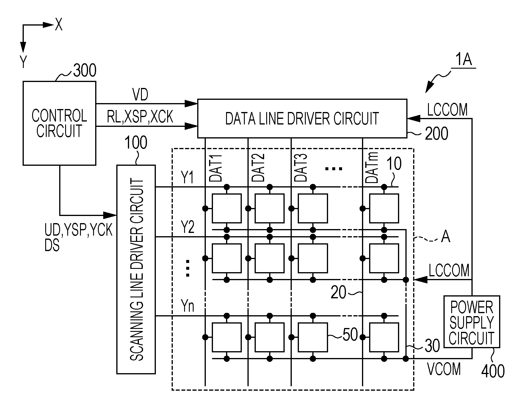
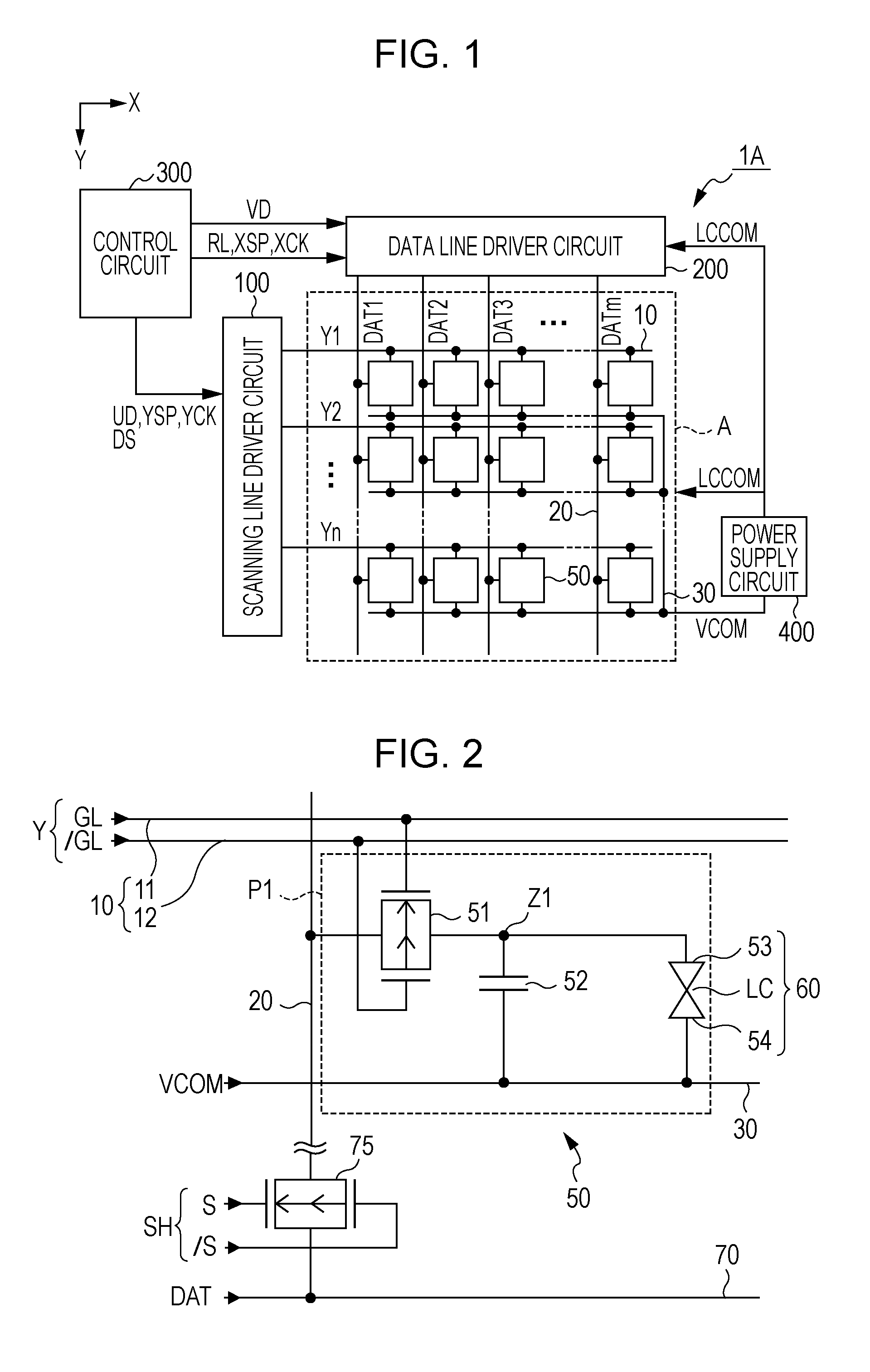
[0053]In the following, the first embodiment according to the invention will be described with reference to FIGS. 1 and 2. Further, in the drawings to be described below including FIGS. 1 and 2 described herein, the dimensions of the respective sections may be different suitably in ratio from the actual ones.

[0054]An electro-optical device according to the embodiment of the invention uses the liquid crystals as an electro-optical material. The electro-optical device 1A includes a liquid crystal panel (which is an example of the electro-optical panel) as a main section. The liquid crystal panel is configured such that an element substrate on which Thin Film Transistors (hereinafter, referred to as “TFT”) are formed and a counter substrate are disposed to face their electrode formed surfaces to each other, and attached with a constant gap therebetween, and then the liquid crystals are interposed in the gap.

[0055]FIG. 1 is a block diagram illustrating the entire configuration of the co...

second embodiment

[0120]In the following, the second embodiment according to the invention will be described with reference to FIG. 10. Further, the second embodiment is characterized in the selection scheme of the scanning lines 10 when the offset potential or the data potential are written, and further points are the same as the configuration, and the operations or the actions of the first embodiment. Therefore, in the following, the differences will be mainly described, and the description of further points will be appropriately simplified, that is, omitted.

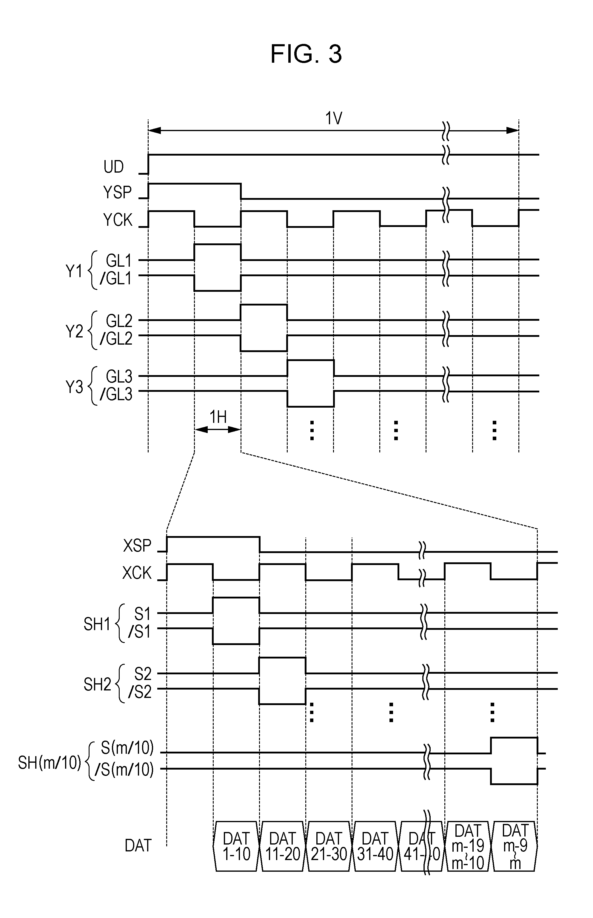
[0121]In the second embodiment, as shown in FIG. 10, the selection scheme of the scanning lines 10 relating to the offset potential and data potential writing operations are different from that of FIG. 7. In other words, in FIG. 10, an inversion function of the Y transfer direction is used, which has been described as a first feature point of the electro-optical device 1A of the first embodiment.

[0122]More specifically, in FIG. 10, when the sel...

third embodiment

[0130]In the following, the third embodiment according to the invention will be described with reference to FIG. 11. Further, the third embodiment is characterized in the selection scheme of the scanning lines 10 when the offset potential or the data potential are written, and further points are the same as the configuration, and the operations or the actions of the first embodiment. Therefore, in the following, the differences will be mainly described, and the descriptions of further points will be appropriately simplified, that is, omitted.

[0131]In the third embodiment, as shown in FIG. 11, the selection schemes of the scanning lines 10 relating to the writing operations of the offset potential and the data potential are different from those of FIGS. 7 and 10.

[0132]More specifically, in FIG. 11, when the selection of all of the scanning lines 10 relating to the offset potential writing operation starts from the first row of the scanning line 10 and is ended at the n-th row of the ...


PUM


Abstract

The electro-optical device includes a first electrode for inverting a polarity, a second electrode opposite to the first electrode, and liquid crystals interposed between these electrodes. Before a polarity inversion timing, the scanning line driver circuit simultaneously selects two or more scanning lines of the plural scanning lines, and the data line driver circuit outputs an offset potential with the polarity opposite to that of the potential of the first electrode thereafter, to a data line. On the other hand, after the polarity inversion timing, the scanning line driver circuit individually selects each of the plural scanning lines, and the data line driver circuit outputs the data potential corresponding to the potential polarity of the first electrode thereafter, to the data line.

Description

TECHNICAL FIELD[0001]The present invention relates to an electro-optical device which includes an electro-optical material such as liquid crystals, and an electronic apparatus which includes the electro-optical device.BACKGROUND ART[0002]As an electro-optical material which varies in its optical characteristics according to electric energy, liquid crystals are known. Liquid crystals vary in their transmittance according to an applied voltage. The variation in the transmittance can be obtained by making the orientation state of the liquid crystal molecules vary according to the applied voltage. In addition, the liquid crystals have a characteristic in which when a direct current voltage is applied for a long time, it is difficult to return the orientation state back to its original state. For this reason, in a liquid crystal display device which is manufactured by applying the liquid crystals to a display device, an alternating current driving that inverts the polarity of the voltage...

Claims


Application Information

Patent Timeline
IPC IPC(8): G09G5/00
CPCG09G3/3614G09G2310/08G09G2310/0283G09G2310/0205
Inventor WATANABE, KENYA
Owner SEIKO EPSON CORP
Why Eureka
Try Eureka