
Methods of Manufacturing Three Dimensional Semiconductor Devices

Inactive Publication Date: 2012-03-22
SAMSUNG ELECTRONICS CO LTD
View PDF2 Cites 129 Cited by
  • Summary
  • Abstract
  • Description
  • Claims
  • Application Information

AI Technical Summary

Benefits of technology

[0005]Example embodiments of the inventive concepts provide methods of easily manufacturing highly integrated three dimensional semiconductor devices.

Problems solved by technology

However, the extremely expensive processing equipment needed to increase pattern fineness sets a practical limitation on increasing integration for two-dimensional or planar semiconductor devices.

Method used


Image

  • Methods of Manufacturing Three Dimensional Semiconductor Devices
  • Methods of Manufacturing Three Dimensional Semiconductor Devices
  • Methods of Manufacturing Three Dimensional Semiconductor Devices

Examples


Embodiment Construction

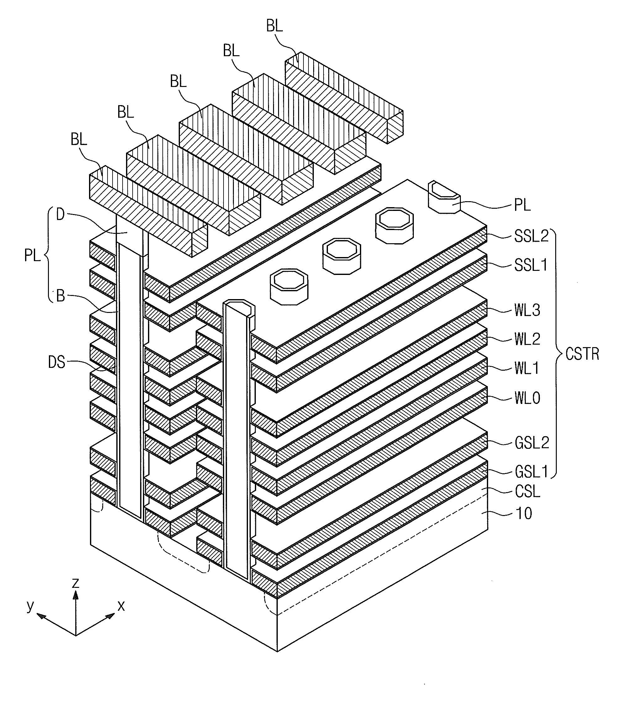
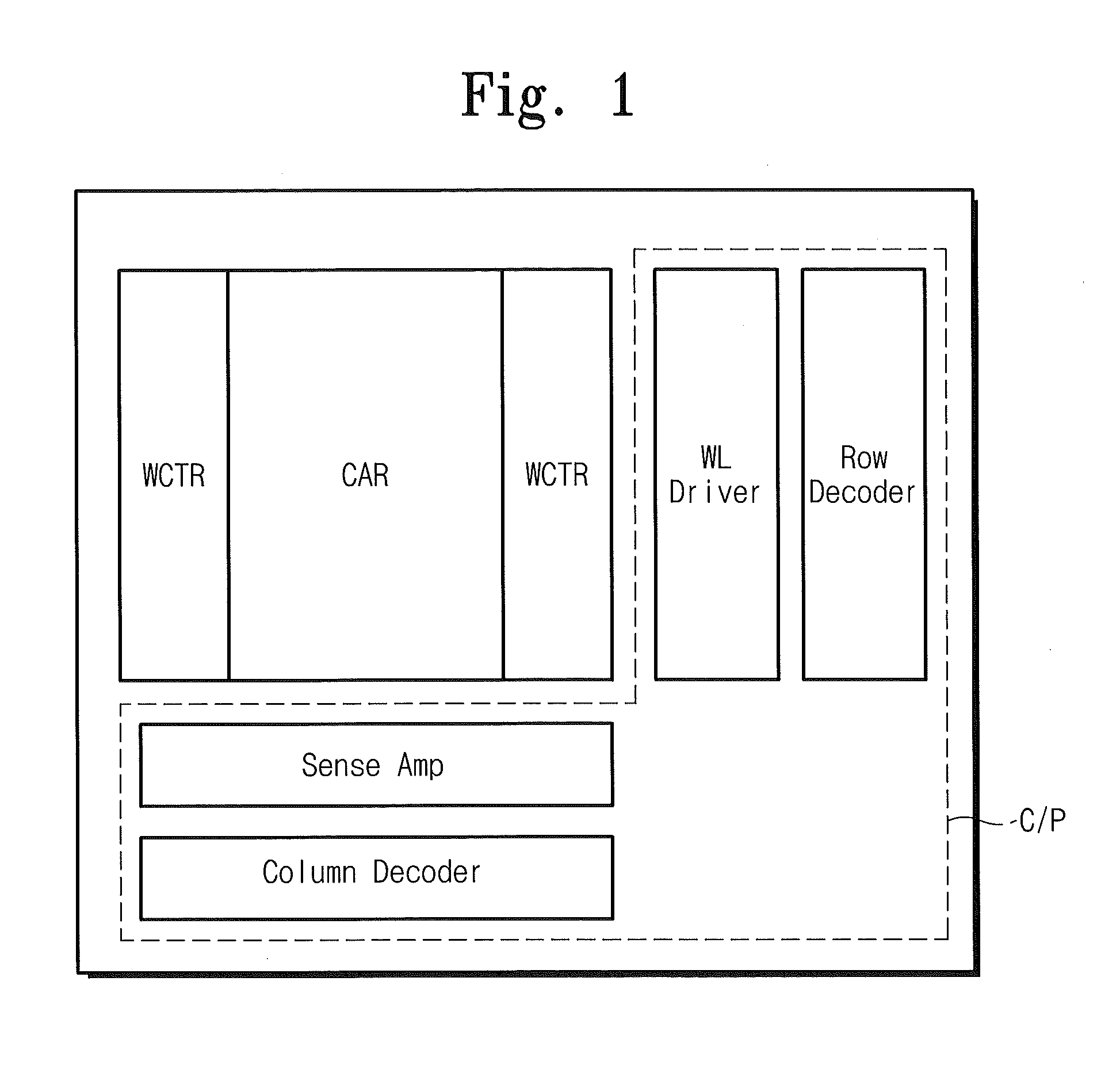
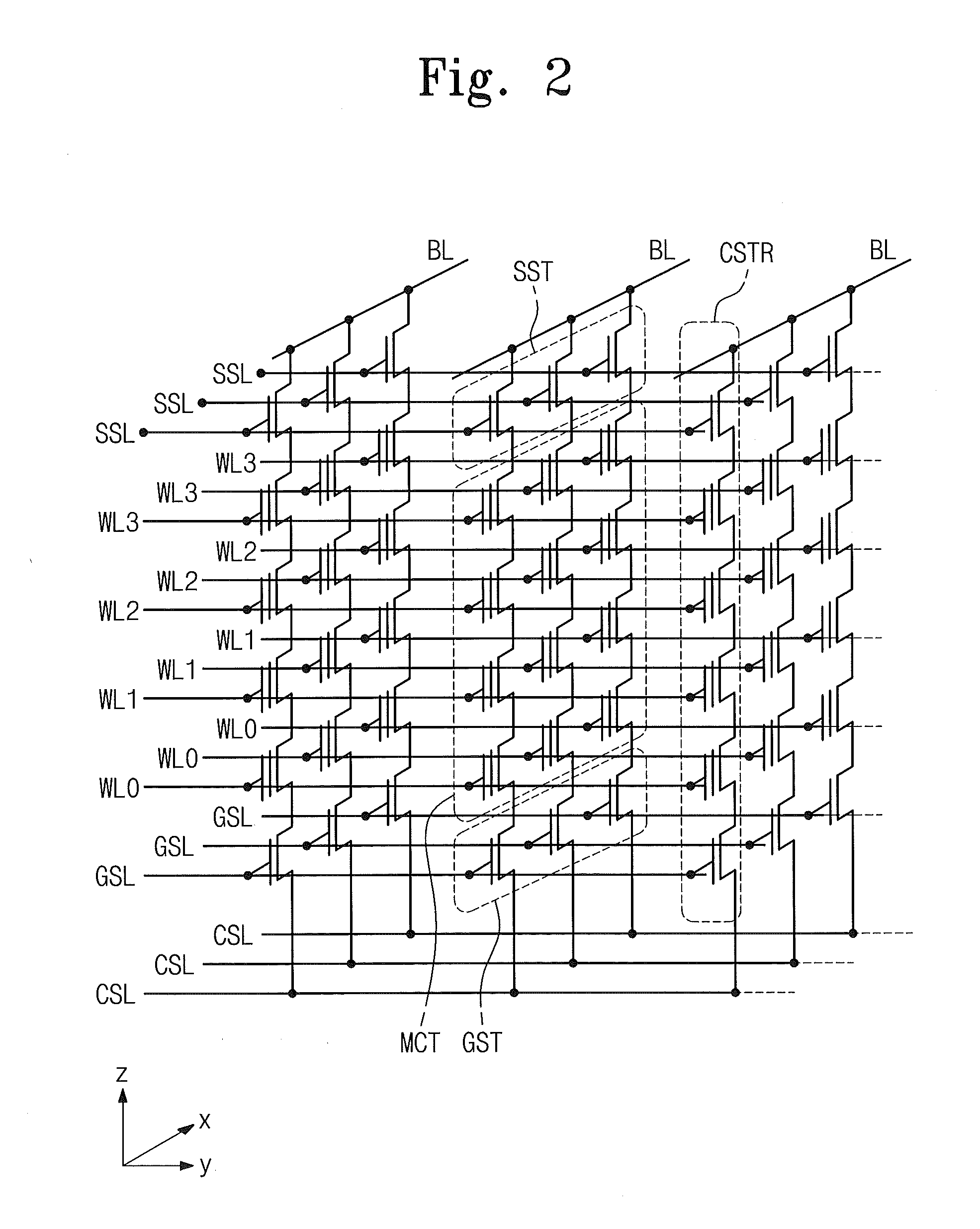
[0024]In a three-dimensional semiconductor memory device, forming a plurality of vertically stacked memory cells in a cell array region may result in a significant height difference between structures in the cell array region and structures in a peripheral circuit region. Thus, an interlayer dielectric formed on both the cell array region and the peripheral circuit region may have a different height (relative to the substrate) in the cell array region than in the peripheral circuit region.

[0025]It may be desirable to planarize the interlayer dielectric to reduce this height difference. However, process control for planarization of an interlayer dielectric may be difficult, resulting in undesirably small process margins. In addition, dishing may occur over the peripheral circuit region and a contact region adjacent the cell array region when planarizing the interlayer dielectric.

[0026]According to example embodiments of the inventive concepts, a polishing stop layer may be selectivel...


PUM


Abstract

Provided are methods of manufacturing a three dimensional semiconductor device. The method includes providing a substrate including a cell array region and a peripheral circuit region, forming a peripheral structure on the peripheral circuit region, forming a cell structure being thicker than the peripheral structure in the cell array region, forming an interlayer dielectric to cover the peripheral structure and the cell structure, forming a polishing stop layer on the interlayer dielectric, and planarizing the interlayer dielectric using the polishing stop layer as a planarization stop.

Description

CROSS-REFERENCE TO RELATED APPLICATIONS[0001]This U.S. non-provisional patent application claims priority under 35 U.S.C. §119 to Korean Patent Application No. 10-2010-0091999, filed on Sep. 17, 2010, in the Korean Intellectual Property Office, the disclosure of which is hereby incorporated by reference.BACKGROUND OF THE INVENTION[0002]Example embodiments of the inventive concepts relate generally to methods of manufacturing a semiconductor device. More particularly, example embodiments of the inventive concepts relate to methods of manufacturing a three dimensional semiconductor device.[0003]Higher integration of semiconductor devices is desired to satisfy consumer demands for superior performance and inexpensive prices for electronic devices. In the case of semiconductor memory devices, since their integration is an important factor in determining product price, increased integration is especially desired. The integration level of typical two-dimensional or planar semiconductor me...

Claims


Application Information

Patent Timeline
IPC IPC(8): H01L21/822
CPCH01L27/0688H01L27/1052H01L27/11582H01L27/11578H10B43/20H10B43/27H01L21/31051H01L29/7926H01L21/822H10B99/00
Inventor KIM, HYU-JUNGPARK, SANG-YONGLIM, JONGHEUNKIM, KYUNGHYUNMUN, CHANGSUP
Owner SAMSUNG ELECTRONICS CO LTD
Learn More