

Electrode plate for plasma etching and plasma etching apparatus
- Summary
- Abstract
- Description
- Claims
- Application Information
AI Technical Summary
Benefits of technology
Problems solved by technology
Method used
Image

Examples
example
Arrangement Example (5)
Arrangement Example Considering Lifespan or Productivity
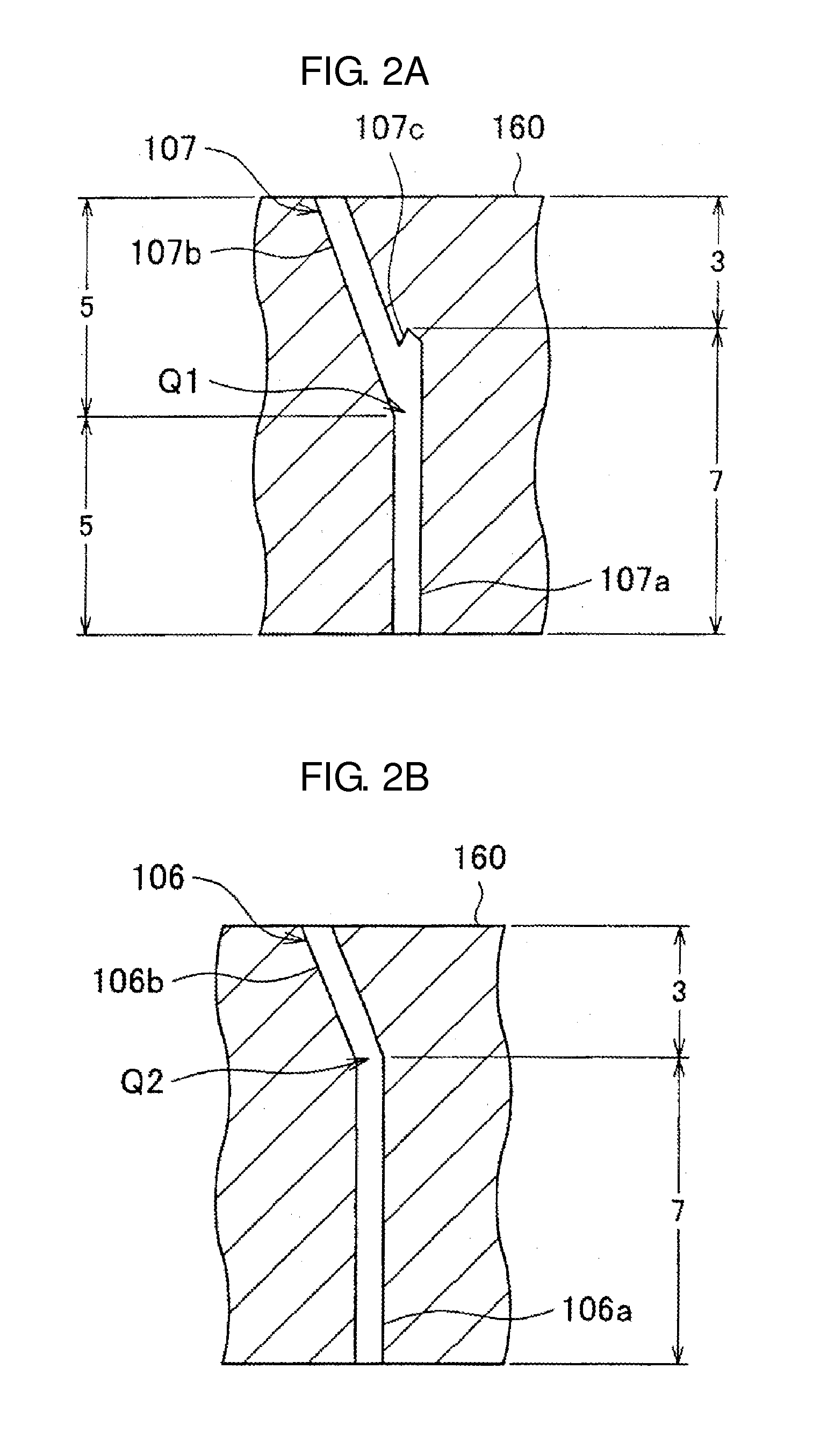
[0090]According to the arrangement example (5), the standard holes are provided in the inner circumferential region, the first inclined holes 106 (7:3) or the standard holes are provided in the intermediate region, and the first inclined holes 106 (7:3) are provided in the outer circumferential region. In the arrangement example (5), the bent holes are provided in the outer circumferential region (and the intermediate region), and thus, the abnormal discharge may be prevented throughout the region where the discharge is most likely to generate. In addition, by providing the standard holes in the inner circumferential region where the discharge hardly generates, the productivity may be improved.
[0091]As described above, the arrangement focusing on preventing the abnormal discharge throughout the region where the discharge is likely to generate and focusing on the amount of abrasion, the productivity, or th...
PUM
| Property | Measurement | Unit |
|---|---|---|
| thickness | aaaaa | aaaaa |
| RF power | aaaaa | aaaaa |
| RF power | aaaaa | aaaaa |
Abstract
Description
Claims
Application Information