Substrate processing apparatus

A substrate processing device and substrate technology, which are applied in the fields of electrical components, semiconductor/solid-state device manufacturing, circuits, etc., can solve problems such as inability to efficiently heat the current gathering ring, and reduced thermal conductivity.

Inactive Publication Date: 2010-12-08
TOKYO ELECTRON LTD
View PDF6 Cites 6 Cited by
  • Summary
  • Abstract
  • Description
  • Claims
  • Application Information

AI Technical Summary

Problems solved by technology

[0006] However, the substrate processing apparatus has a structure in which a plurality of components are combined, and since the gap between the components functions as a vacuum insulation layer, the thermal conductivity is reduced. In conventional substrate processing apparatuses equipped with embedded heaters, each The components, especially the collector ring and its peripheral parts cannot be heated efficiently

Method used


Image

  • Substrate processing apparatus
  • Substrate processing apparatus
  • Substrate processing apparatus

Examples


Embodiment Construction

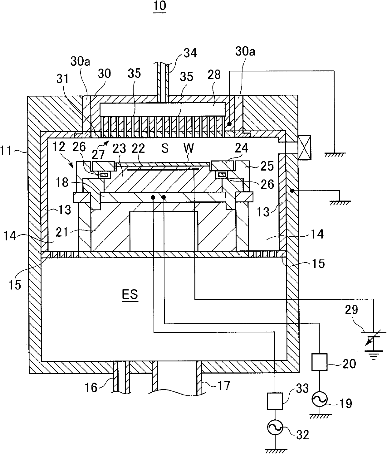
[0038] Below, refer to the attached Figure one The first embodiment of the present invention will be described in detail.

[0039] figure 1 It is a cross-sectional view schematically showing the configuration of the substrate processing apparatus according to the first embodiment of the present invention. This substrate processing apparatus is configured to perform RIE (Reactive Ion Etching) processing on a semiconductor wafer W as a substrate.

[0040] in figure 1 Among them, the substrate processing apparatus 10 has a cylindrical processing chamber 11 having a processing space S above the inside. The plasma described later is generated in the processing space S. In the processing chamber 11, a cylindrical susceptor 12 is arranged as a substrate mounting table on which a semiconductor wafer W (hereinafter, simply referred to as "wafer W") having a diameter of, for example, 300 mm is mounted. The inner wall surface of the processing chamber 11 is covered with a side wall member...


PUM


Abstract

Provided is a substrate processing apparatus capable of effectively heating each component without generating an abnormal electric discharge. The substrate processing apparatus 10 includes: a depressurizable processing chamber 11; a susceptor 12 provided within the processing chamber 11; a shower head 27 provided at a ceiling portion of the processing chamber 11 so as to face the susceptor 12; a focus ring 24 provided at an outer peripheral portion of a top surface of the susceptor 12; and a ring-shaped infrared radiant heater 26 provided in a vicinity of the focus ring 24. The heater 26 includes an infrared radiator 26a and a quartz ring 26b for sealing the infrared radiator 26a therein so that there is not a member for blocking the infrared radiation between the focus ring 24 and the heater 26.

Description

Technical field [0001] The present invention relates to a substrate processing apparatus, and in particular to a substrate processing apparatus in which a heater is provided in the processing chamber to eliminate the main factors hindering substrate processing. Background technique [0002] Examples of substrate processing apparatuses include semiconductor manufacturing apparatuses, vacuum processing apparatuses, and film forming processing apparatuses. As substrate processing apparatuses that process substrates using plasma, plasma processing apparatuses are known. The plasma processing apparatus has a decompressible processing chamber (chamber) that generates plasma inside, and a substrate mounting table (susceptor) on which a wafer as a substrate is placed is arranged in the chamber. The base includes a disc-shaped electrostatic chuck (ESC) arranged on the upper surface of the base, and a converging ring made of silicon, for example, arranged on the outer peripheral edge of th...

Claims


Application Information

Patent Timeline
Patent Type & Authority Applications(China)
IPC IPC(8): H01L21/00
CPCH01L21/67103H01L21/67115H01L21/68714
Inventor 饭塚八城望月祐希
Owner TOKYO ELECTRON LTD
Why Eureka
Try Eureka