Display device

a technology of a display device and a display screen, which is applied in the direction of thermoelectric device junction materials, semiconductor devices, electrical apparatus, etc., can solve the problems of difficult control of the film thickness of the organic compound layer constituting, difficult to form the organic el element, and different white color chromaticity, so as to reduce the brightness and reduce the brightness. small, the effect of large brightness reduction

Inactive Publication Date: 2012-03-29
CANON KK
View PDF1 Cites 8 Cited by
  • Summary
  • Abstract
  • Description
  • Claims
  • Application Information

AI Technical Summary

Benefits of technology

[0069]As described above, the radiation characteristics can be controlled by a method different from the methods of the first embodiment to the third embodiment. For example, when the radiation characteristics are controlled by a region occupied by the lens of the pixel region, the effects of the invention are demonstrated in the case of the following configuration. More specifically, the region occupied by the lens may be enlarged in a pixel having an organic EL element with low angular dependence of brightness and the region occupied by the lens may be reduced in a pixel having an organic EL element with high angular dependence of brightness. Due to the configuration, the ratio of light beams that penetrate the lens among light beams emitted from the light emitting regions (pixels) can be adjusted, and thus the radiation characteristics of the entire pixel are controlled.
[0070]Moreover, in the configuration described above, the lens is provided in accordance with the angular dependence of brightness of color in which the reduction in the brightness is small. However, even in a configuration such that the lens is provided in accordance with the angular dependence of brightness of color in which the reduction in the brightness is large, the white color shift can be reduced. Specifically, the following configuration is mentioned.
[0071]More specifically, the radiation characteristics can also be adjusted by providing both a configuration such that a concave lens is provided and a configuration in which a convex lens is provided. The radiation characteristics of the convex lens are lower and the light gathering characteristics thereof are higher than the configuration in which a concave lens is provided and than the configuration in which no lenses are provided. By utilizing the characteristics, a convex lens may be provided in a pixel having an organic EL element with low angular dependence of brightness and a concave lens may be provided in a pixel having an organic EL element with high angular dependence of brightness.
[0072]The radiation characteristics (light gathering characteristics) of pixels can also be controlled only by a convex lens by utilizing the fact that, in the convex lens, the radiation characteristics become lower as the radius of curvature becomes lower (the light gathering characteristics become higher). More specifically, it may be configured such that a convex lens with a small radius of curvature is provided in a pixel having an organic EL element with low angular dependence of brightness and a convex lens with a large radius of curvature is provided in a pixel having an organic EL element with high angular dependence of brightness. Even in the configuration, the difference of the angular dependence of brightness of the organic EL elements of the respective colors can be made small.
[0073]Mentioned as the display device of the invention are television sets, personal computers, imaging devices, display portions of cellular phones, and portable game machines. In addition, portable music playback devices, Personal Digital Assistant (PDA), car navigation systems, and the like are mentioned.EXAMPLES

Problems solved by technology

However, since the organic EL elements of the respective colors (red, green, and blue) are different from each other in the angular dependence of brightness, there has been a problem in that the white color chromaticity is different between the case where the display device is observed from the front and the case where the display device is observed at an angle inclining from the front (white color shift).
However, it is difficult to control the film thickness of the organic compound layer constituting the organic EL element and it is difficult to form the organic EL element as designed while suppressing the in-plane variation of the functional layers which are thin films and further considering the interference.

Method used


Image

  • Display device
  • Display device
  • Display device

Examples


first embodiment

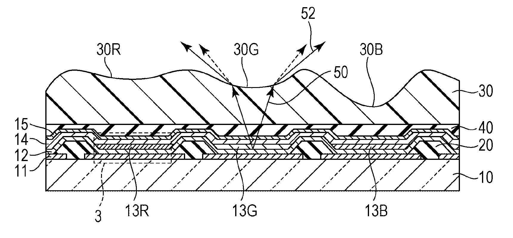
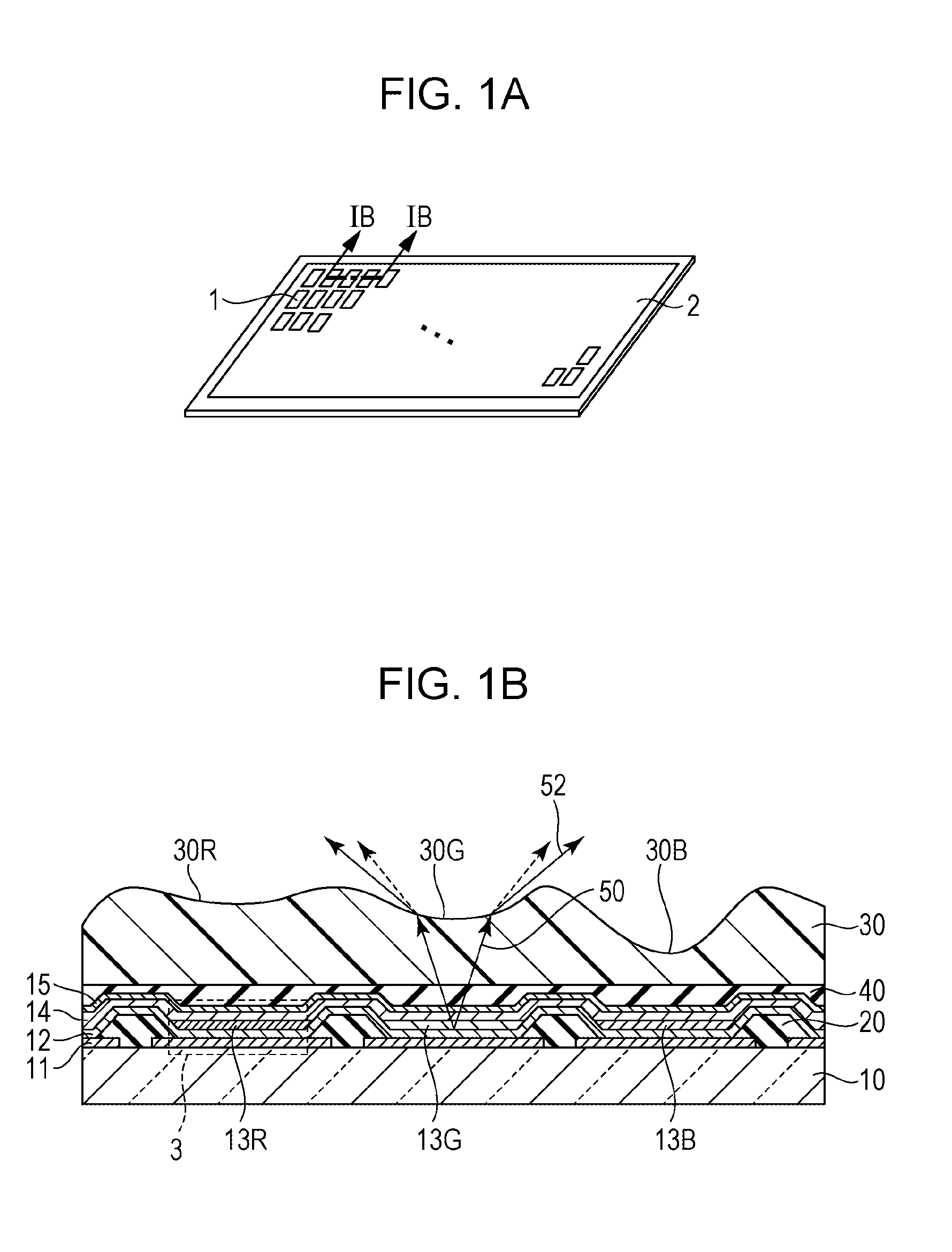
[0022]FIG. 1A is a perspective schematic view illustrating a display device according to a first embodiment of the invention. The display device of this embodiment has two or more pixels 1 each having an organic EL element. The two or more pixels 1 are disposed in the shape of a matrix and form a display region 2. The pixel refers to a region corresponding to a light emitting region of one light emitting element. In the display device of this embodiment, the light emitting element is an organic EL element and the display device of this embodiment is a display device in which an organic EL element of one color is disposed in each of the pixels 1. As the emission color of the organic EL elements, red, green, and blue can be considered and, in addition, yellow, cyan, and white may be acceptable. The color is not particularly limited insofar as at least two or more colors are employed. In the display device of this embodiment, two or more pixel units containing two or more pixels differ...

second embodiment

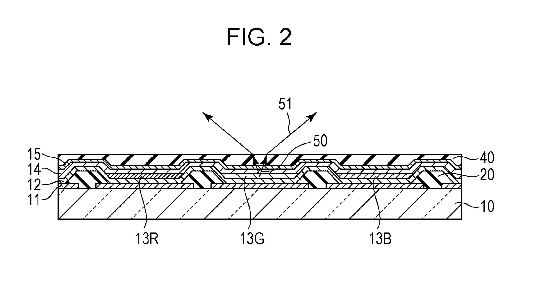
[0060]FIG. 5 is a partial sectional schematic view of a display device of this embodiment. The first embodiment relates to the display device in which the radius of curvature of the lenses is varied in the organic EL elements of the respective colors to thereby control the radiation characteristics, whereby the difference in the angular dependence of brightness of the organic EL elements of the respective colors is made small. In contrast, this embodiment relates to a display device in which the distance between a lens and a light emitting layer of each organic EL element is varied in the organic EL elements of the respective colors to thereby control the radiation characteristics, whereby the difference in the angular dependence of brightness of the organic EL elements of the respective colors is made small.

[0061]In general, the radiation characteristics of the lens become small with an increase in the distance between the concave lens and the light emitting point (or light emittin...

example 1

[0074]This Example describes an example in which the difference of the angular dependence of brightness of organic EL elements using lenses different in the radius of curvature will be described with reference to FIGS. 4A to 4E.

[0075]First, a low-temperature polysilicon TFT was formed on a glass substrate, and then an interlayer insulation film containing nitride silicon and a planarization film containing acrylic resin were formed thereon in this order, thereby creating a substrate 10 illustrated in FIG. 4A. An ITO film / AlNd film was formed on the substrate 10 by sputtering with a thickness of 38 nm / 100 nm. Subsequently, the ITO film / AlNd film was patterned for every pixel to form first electrodes 11.

[0076]Acrylic resin was applied onto the first electrodes 11 by spin coating. The acrylic resin was patterned by lithography in such a manner that openings (the openings correspond to the pixels) were formed in portions where the first electrodes 11 were formed to thereby form an insul...


PUM


Abstract

A pixel unit having two or more pixels different in emission color is provided with lenses in such a manner that the difference of the angular dependence of brightness in organic EL elements for every emission color of the pixels becomes small.

Description

BACKGROUND OF THE INVENTION[0001]1. Field of the Invention[0002]The present invention relates to a display device having organic EL elements.[0003]2. Description of the Related Art[0004]In recent years, the display device having organic EL elements has been actively researched and developed. The organic EL element is constituted by an anode, an organic compound layer containing a light emitting layer, and a cathode, in which a hole and an electron are injected into the light emitting layer from the anode and the cathode, respectively, so that a light beam is emitted from the light emitting layer utilizing the recombination energy of the hole and the electron.[0005]In order to achieve color display, a display device having two or more organic EL elements that emit different colors of red, green, and blue, for example, displays white color by making the organic EL elements of the respective colors emit a light beam. However, since the organic EL elements of the respective colors (red,...

Claims


Application Information

Patent Timeline
Patent Type & Authority Applications(United States)
IPC IPC(8): H01L27/32
CPCH01L51/5275H10K50/858
Inventor SUMIDA, NOASAKAGUCHI, KIYOFUMIHASEGAWA, TOSHINORIMATSUDA, YOJIRO
Owner CANON KK
Why Eureka
Try Eureka