Method to measure 3 component of the magnetic field vector at nanometer resolution using scanning hall probe microscopy

a scanning hall probe and magnetic field technology, applied in the field of measuring the 3 component of the magnetic field vector at nanometer resolution, can solve the problems of difficult assembling of parts, the integration of ohmic contacts, and the inability of the electron to overcome the potential barrier, and achieve high spatial resolution

Inactive Publication Date: 2012-03-29
ORAL AHMET +2
View PDF5 Cites 3 Cited by
  • Summary
  • Abstract
  • Description
  • Claims
  • Application Information

AI Technical Summary

Benefits of technology

[0023]It is an advantage of the invention that the sample to be imaged does not require any special sample preparation.
[0024]It is a further advantage of the invention is that the spatial resolution is defined by the spatial resolution of the single sensor used and is improved considerably compared to other existing prior methods.
[0025]It is a further advantage of the invention is that 3 component of the magnetic field vector at nanometer resolution measuring method needs limited amount of data analysis.
[0026]It is a further advantage of the invention is that 3 component of the magnetic field vector at nanometer resolution measuring method is much faster.
[0027]It is a further advantage of the invention is that 3 component of the magnetic field vector at nanometer resolution measuring method and scanning hall probe microscopy can be applied in variable temperature environments in external magnetic field.
[0028]In Scanning Hall Probe Microscopy, a Hall probe integrated with an STM tip is brought in to close proximity of the sample under inspection using the course approach mechanism. The sample is tilted 1-20 about the probe to have the STM tip at the highest position. Integrated STM tip keeps track of the surface just like in the case of STM seeking a tunneling current. The tunneling current is fed into a control electronic to maintain a constant current changing the height of the sensor with respect to the topography of the sample using a piezo tube scanner. This simultaneous topography and magnetic imaging can be accomplished while scanning the designated area within the scan range of the piezo. Overall control of approach and scan is maintained via dedicated SHPM control electronics. It is also possible to use AFM feedback which makes it possible to scan non-conductive samples for simultaneous topography and magnetic data. The technique can give quantitative data with high spatial resolution. Microscope can work in a wide temperature range under high magnetic fields.

Problems solved by technology

Classically electrons are not expected to overcome the potential barrier.
Although it is possible to get information about the magnetic properties of the materials with macroscopic measurements, it is only possible to interpret them further with the aid of local measurement techniques done at the macroscopic level.
The difficulty about the integration was the placement of the ohmic contacts for each pad forming the Hall element.
Since the assembling the parts is difficult, alignment and angle errors may arise.
Also, due to the huge measurement volume, local measurements are difficult and some corrections have to be applied to the acquired data.
The main problem with this layout, reported by different groups, is the cross coupling between XYZ channels.

Method used


Image

  • Method to measure 3 component of the magnetic field vector at nanometer resolution using scanning hall probe microscopy
  • Method to measure 3 component of the magnetic field vector at nanometer resolution using scanning hall probe microscopy
  • Method to measure 3 component of the magnetic field vector at nanometer resolution using scanning hall probe microscopy

Examples


Embodiment Construction

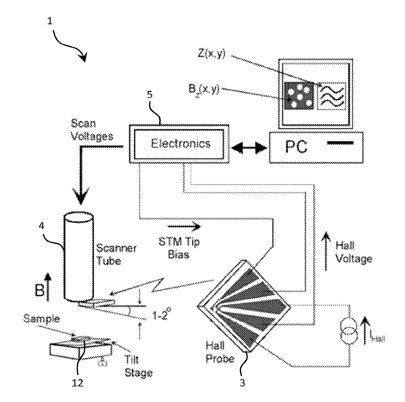
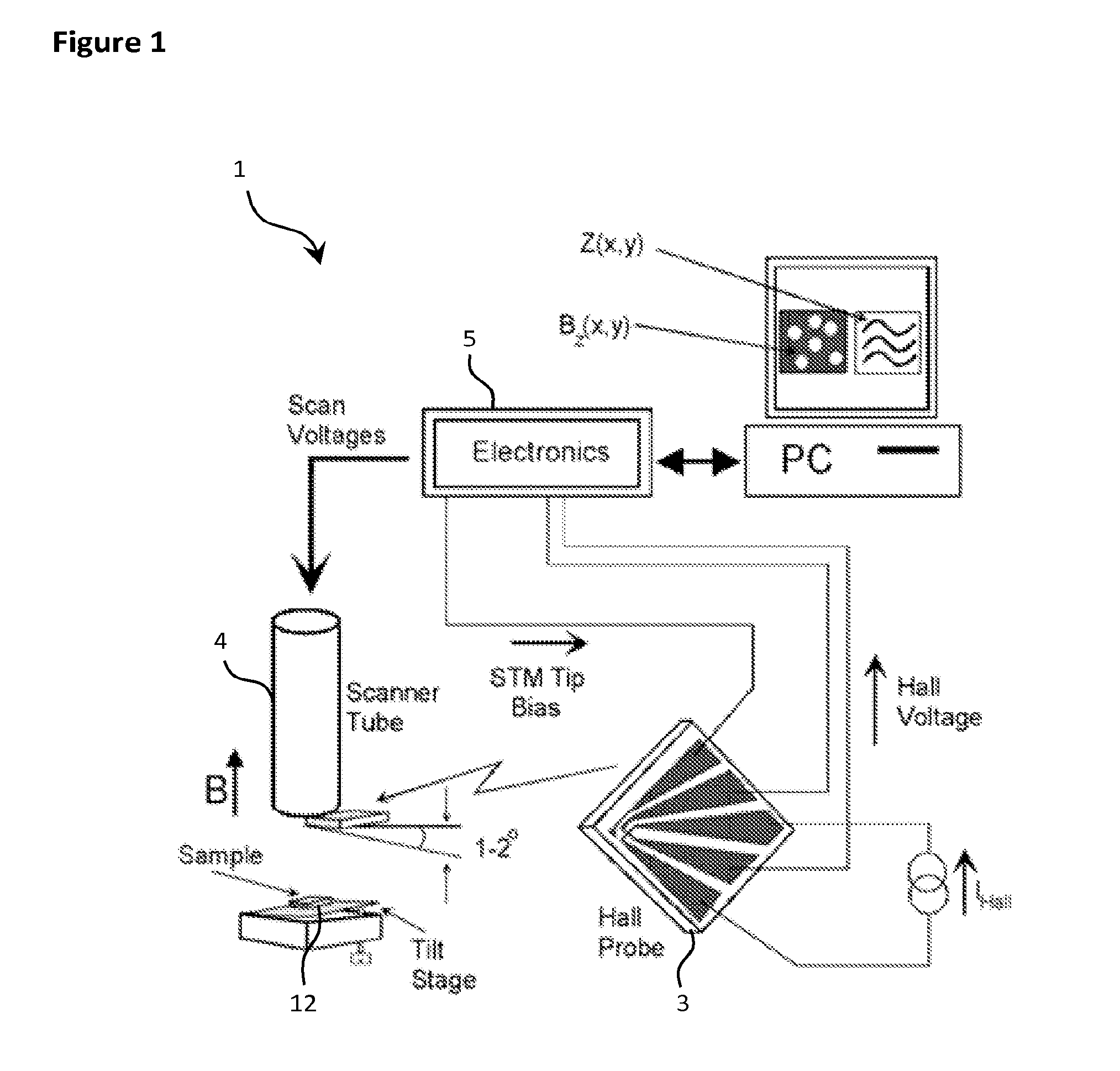
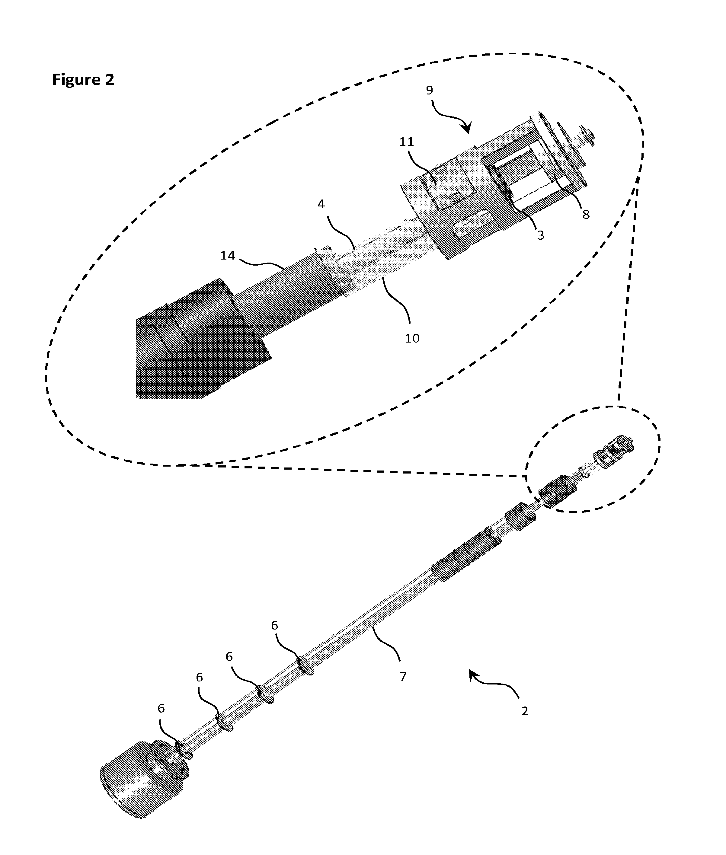
[0040]The scanning hall probe microscope (SHPM) (1) includes; a microscope body (2), a hall probe (3), an approach mechanism, a scanner (4) and control electronics (5).

[0041]The microscope body (2) is an assembly housing all the mechanical parts, moving or stationary, which forms the microscope (1). The microscope body (2) preferably has a compact form in order to fit in to cryostat systems for low temperature applications. Moreover it includes radiation baffles (6), extension tube (7), sample holder (8), slider puck (9), slider tube (10), leaf spring (11) and hollow cylindrical shield. Radiation baffles (6) decrease the effect of the radiation from high temperature and help preserve the cryogen. The extension tube (7) is designed to bring the scanner head to the magnet center of the cryostat. It also houses the cables used for carrying signals. The sample (12) is placed on the sample holder (8) facing towards the sensor, which is mechanically attached to the slider puck (9). The pu...


PUM


Abstract

Scanning hall probe microscopy is used to measure 3 components of the magnetic field vector at nanometer resolution by connecting of Hall probe to the end of the piezo scanner, then gluing of the sample to the sample holder, thereafter positioning of the SHPM head under the optical microscope with approximately X40 magnification, then moving back of the slider puck around approximately 30 steps or moving the sensor or sample back by suffient amount using motors, piezo or other positioner such that signal decays to negligible levels; thereafter setting the temperature of cryostat or to desired temperature, then offset nulling of the Hall sensor in gradiometer or normal conditions, and finally setting of the scan area, speed, resolution and the acquisition channels through SPM control program.

Description

BACKGROUND OF THE INVENTION[0001]1. Field of the Invention[0002]This invention relates to a method to measure 3 component of the magnetic field vector at nanometer resolution using scanning hall probe microscopy.[0003]2. Description of the Related Art[0004]The history of the Scanning Probe Microscopes (SPMs) started with the invention of Scanning Tunneling Microscope (STM) in 1981 by Binnig and Rohrer. In this technique an atomically sharp conductive tip is brought in to close proximity of a conductive sample. Classically electrons are not expected to overcome the potential barrier. But it is known, from quantum mechanics, that there exist a non zero possibility for electrons to tunnel the air or vacuum gap between the tip and the sample. The tunneling current is exponential function of the height of the tip over the sample. Thus, if the current is fed into a control circuit it is possible to control the height of the tip. By this way a sample surface could be scanned with atomic re...

Claims


Application Information

Patent Timeline
Patent Type & Authority Applications(United States)
IPC IPC(8): G01Q10/00G01Q60/00
CPCG01Q60/54B82Y35/00
Inventor ORAL, AHMETDEDE, MUNIRARKAM, RIZWAN
Owner ORAL AHMET
Why Eureka
Try Eureka