Multilayer ceramic electronic components and method of manufacturing the same

Inactive Publication Date: 2012-04-26
SAMSUNG ELECTRO MECHANICS CO LTD
View PDF3 Cites 16 Cited by
  • Summary
  • Abstract
  • Description
  • Claims
  • Application Information

AI Technical Summary

Benefits of technology

[0010]An aspect of the present invention provides a multilayer ceramic electronic component having excellent reliability while resisting thermal impact cracks by having the

Problems solved by technology

However, as the thickness of dielectric and inner electrode layers is reduced, the thickness of inner electrode layers becomes non-uniform and the inner elect

Method used


Image

  • Multilayer ceramic electronic components and method of manufacturing the same
  • Multilayer ceramic electronic components and method of manufacturing the same
  • Multilayer ceramic electronic components and method of manufacturing the same

Examples


Example

[0021]Hereinafter, exemplary embodiments of the present invention will be described in detail with reference to the accompanying drawings, which will fully convey the concept of the invention to those skilled in the art. Moreover, detailed descriptions related to well-known functions or configurations will be ruled out in order not to unnecessarily obscure the subject matter of the present invention. It is also noted that like reference numerals denote like elements in appreciating the drawings.

[0022]Exemplary embodiments of the present invention will now be described in detail with reference to the accompanying drawings.

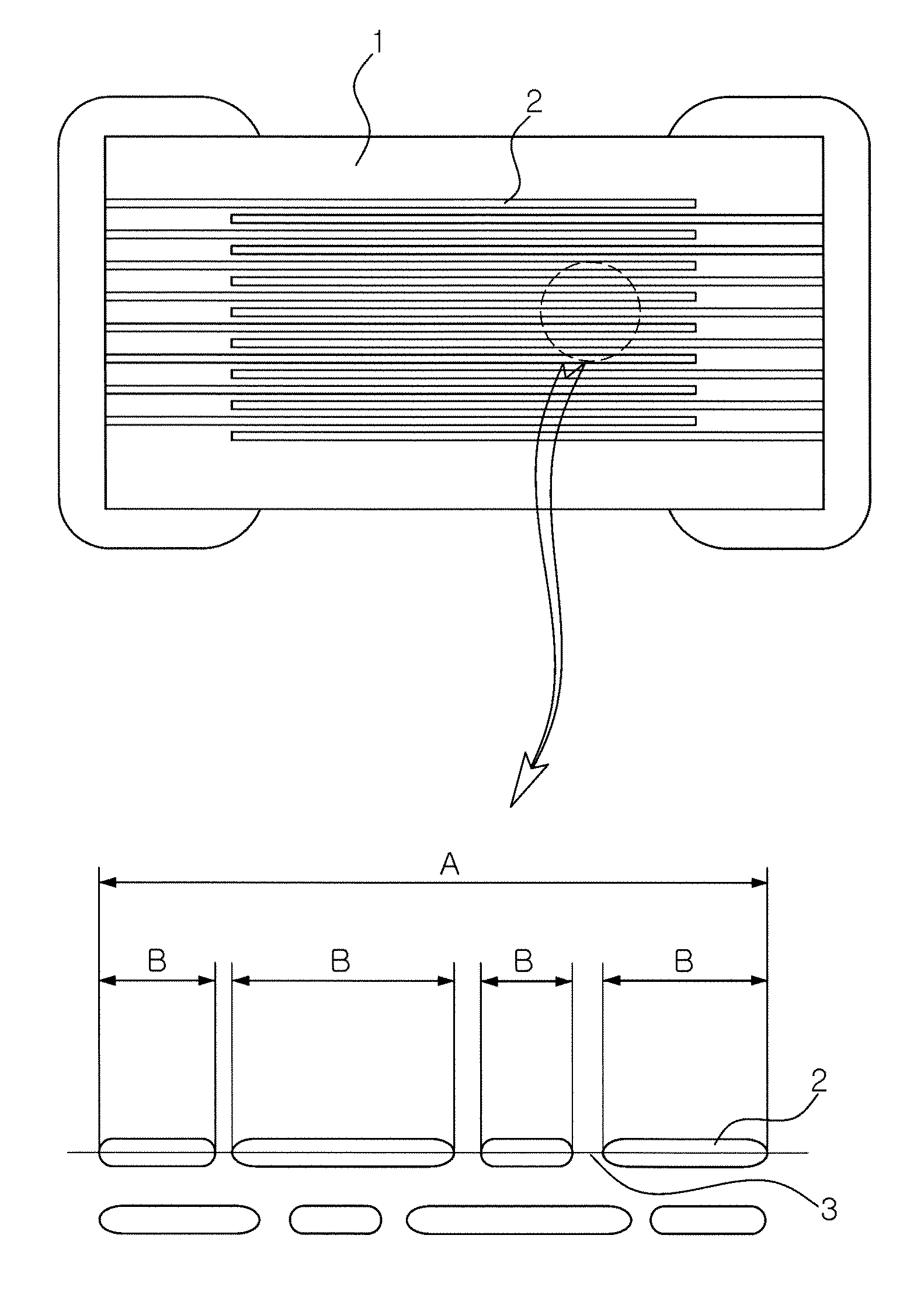
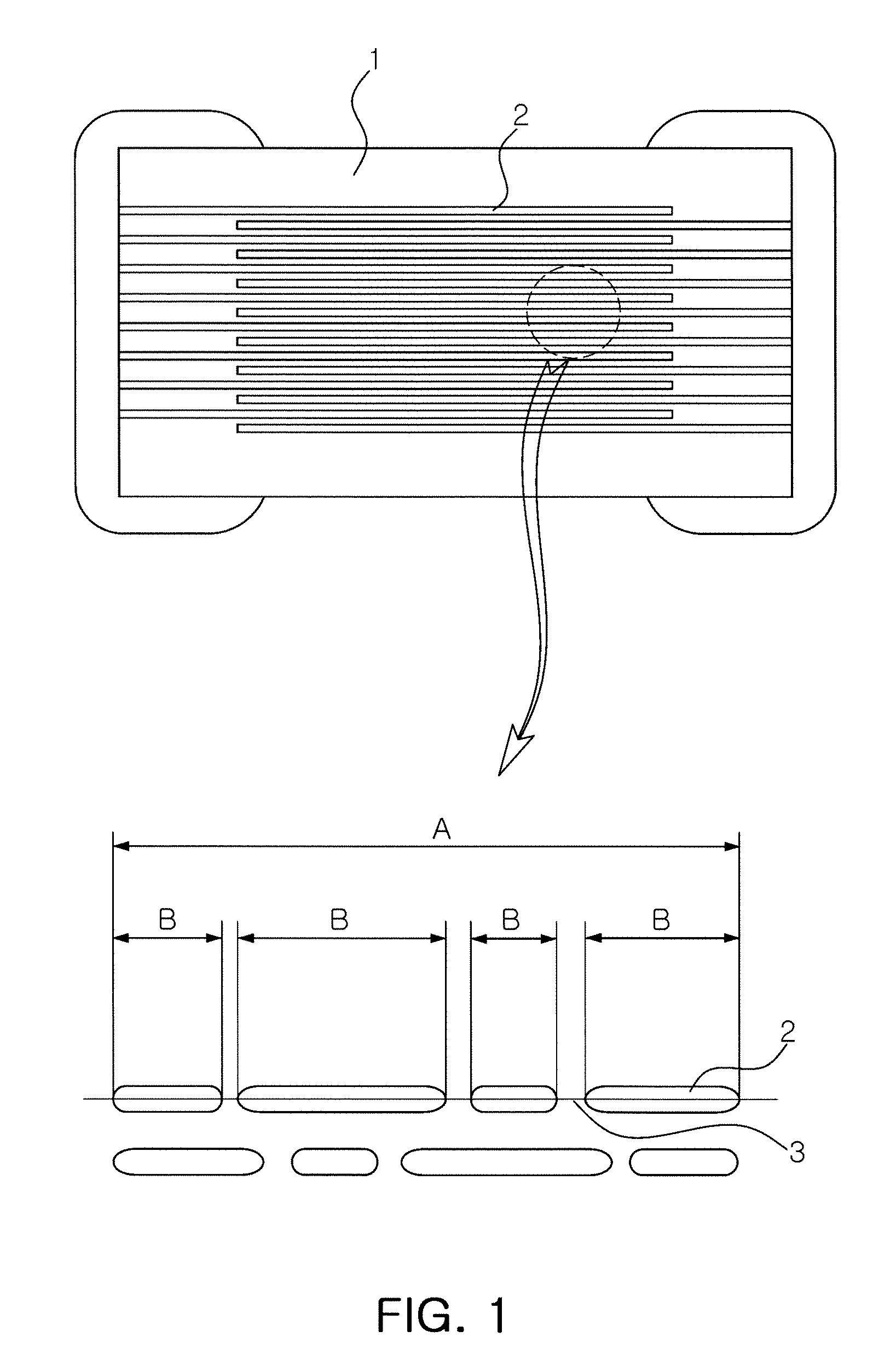
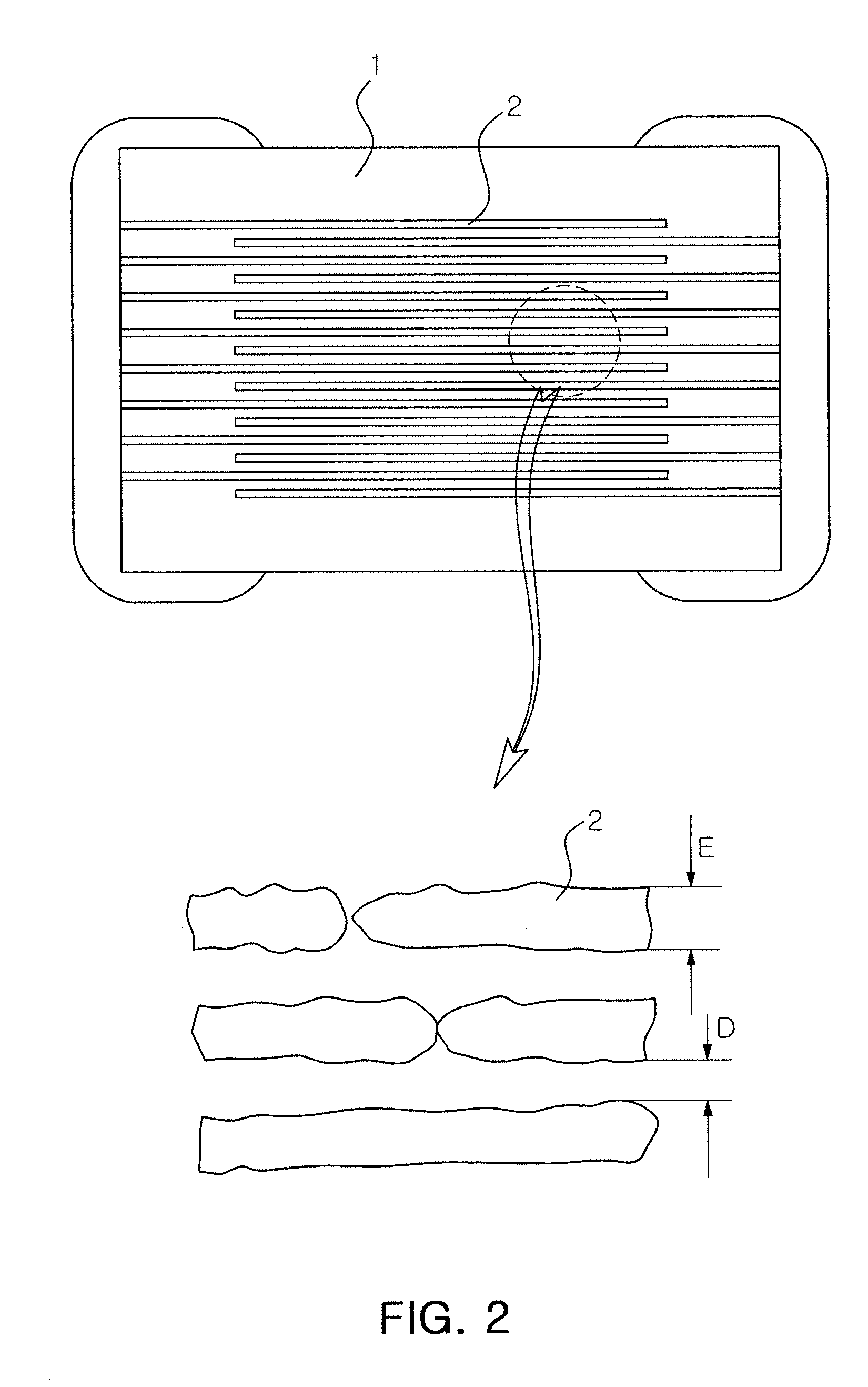
[0023]FIG. 1 illustrates a cross-sectional view and an enlarged view schematically showing multilayer ceramic electronic component.

[0024]The connectivity B / A of the inner electrode layer may be defined by a ratio of an actual total length B of a cross section applied with an inner electrode to a total length A of a cross section of an inner electrode. That is, the c...


PUM

PropertyMeasurementUnit
Lengthaaaaaaaaaa
Fractionaaaaaaaaaa
Percent by massaaaaaaaaaa

Abstract

Disclosed are a multilayer ceramic electronic component and a method of manufacturing the same. There is provided a multilayer ceramic electronic component, including: a ceramic main body in which a plurality of dielectric layers having an average thickness of 1 μm or less are stacked; and inner electrode layers formed on the dielectric layers and having connectivity of 90% or more expressed by the following Equation, wherein the ratio of the thickness of the inner electrode layer to the thickness of the dielectric layer is between 0.8:1 and 1.3:1. The Equation is as follows.
CONNECTIVITY=TOTALLENGTH(B)OFCROSSSECTIONFORMEDWITHCONDUCTIVEPASTETOTALLENGTH(A)OFCORSSSECTIONOFINNERELECTRODE
The high-capacity multilayer ceramic electronic component having the excellent reliability while resisting the thermal impact cracks can be provided, by having the uniform thickness of the dielectric layers to improve the voltage-resistant characteristics while implementing the high capacitance.

Description

CROSS-REFERENCE TO RELATED APPLICATIONS[0001]This application claims the priority of Korean Patent Application No. 2010-0104836 filed on Oct. 26, 2010, in the Korean Intellectual Property Office, the disclosure of which is incorporated herein by reference.BACKGROUND OF THE INVENTION[0002]1. Field of the Invention[0003]The present invention relates to multilayer ceramic electronic components and a method of manufacturing the same, and more particularly, to multilayer ceramic electronic components having excellent reliability and resistance to thermal impact cracks, and a method of manufacturing the same.[0004]2. Description of the Related Art[0005]Generally, a multilayer ceramic capacitor (MLCC) is a chip-type condenser mounted on a printed circuit board for use in various electronic products such as mobile communications terminals, notebook (or laptop) computers, desktop computers, personal digital assistants (PDA), and the like, to perform an important role in storing and dischargi...

Claims


Application Information

Patent Timeline
IPC IPC(8): H01G4/30H01G7/00H01B1/22H01G4/12H01G4/232H01G13/00
CPCH01G4/012Y10T29/43H01G4/30
Inventor CHANG, DONG IKHUR, KANG HEONKIM, DOO YOUNGJEONG, JI HUN
Owner SAMSUNG ELECTRO MECHANICS CO LTD
Why Eureka
Try Eureka