Transistor and method for forming the same

Active Publication Date: 2012-05-03
INST OF MICROELECTRONICS CHINESE ACAD OF SCI
View PDF2 Cites 19 Cited by
  • Summary
  • Abstract
  • Description
  • Claims
  • Application Information

AI Technical Summary

Benefits of technology

[0018]According to the present invention, due to the fact that one or more dislocations are formed only in the source region, the junction leakage is less likely to increase while the electron mobility in the channel region can be increased.

Problems solved by technology

However, if a dislocation is formed in the drain region, junction leakage will increase due to the voltage difference between the drain and the substrate.

Method used


Image

  • Transistor and method for forming the same
  • Transistor and method for forming the same
  • Transistor and method for forming the same

Examples


first embodiment

The First Embodiment

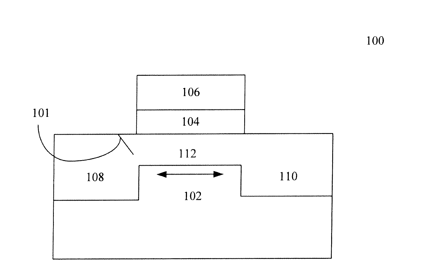
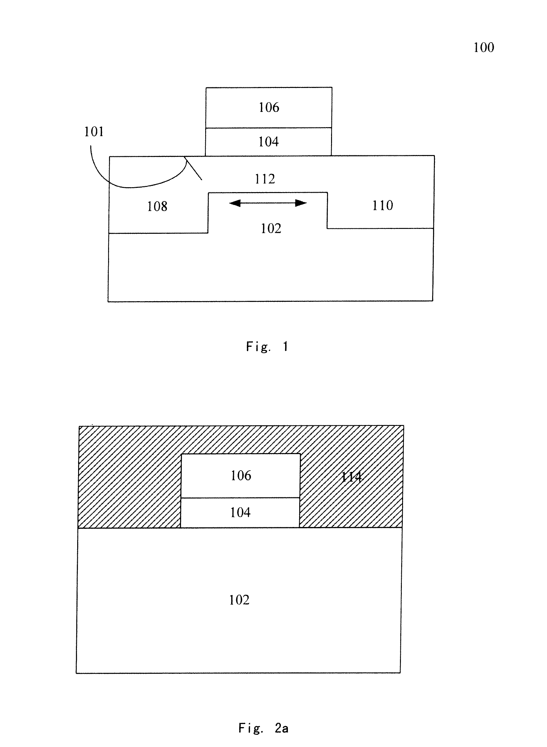
[0033]FIG. 1 schematically illustrates a transistor according to the first embodiment of the present invention. As shown in FIG. 1, a transistor 100 comprises a semiconductor substrate 102, a gate dielectric layer 104 formed on the semiconductor substrate 102, a gate 106 formed on the gate dielectric layer 104, a source region 108 and a drain region 110 in the semiconductor substrate 102 and on respective sides of the gate 106, and a channel region 112 under the gate dielectric layer 104 and between the source region 108 and the drain region 110. In the transistor 100 shown in FIG. 1, the source region 108 comprises a dislocation 101 adjacent to the channel region 112. The dislocation 101 applies tensile stress (as indicated by the arrow in the figure) to the channel region 112, which increases the electron mobility in the channel region.

[0034]In addition, the transistor 100 further comprises sidewall spacers formed on the side surfaces of the gate dielectric lay...

second embodiment

The Second Embodiment

[0039]FIG. 3 schematically shows a transistor according to the second embodiment of the present invention. The transistor 200 shown in FIG. 3 is different from the transistor 100 shown in FIG. 1 in that there are two dislocations in the source region 108 in the direction parallel to a top surface of the substrate 102. Although the dislocations are shown not to intersect each other in FIG. 3, the dislocations may intersect each other.

[0040]The method for forming the transistor 200 is similar to that for forming the transistor 100. First, a mask layer 114 is formed on a semiconductor substrate 102 on which a gate dielectric layer 104 and a gate 106 have been formed, so that the mask layer 114 covers the gate 106 and the semiconductor substrate 102, which is the same as the step shown in FIG. 2a of the first embodiment and thus is not shown here. Next, the mask layer 114 is patterned so that only a portion of the source region 108 is exposed, as shown in FIG. 4a. P...

third embodiment

The Third Embodiment

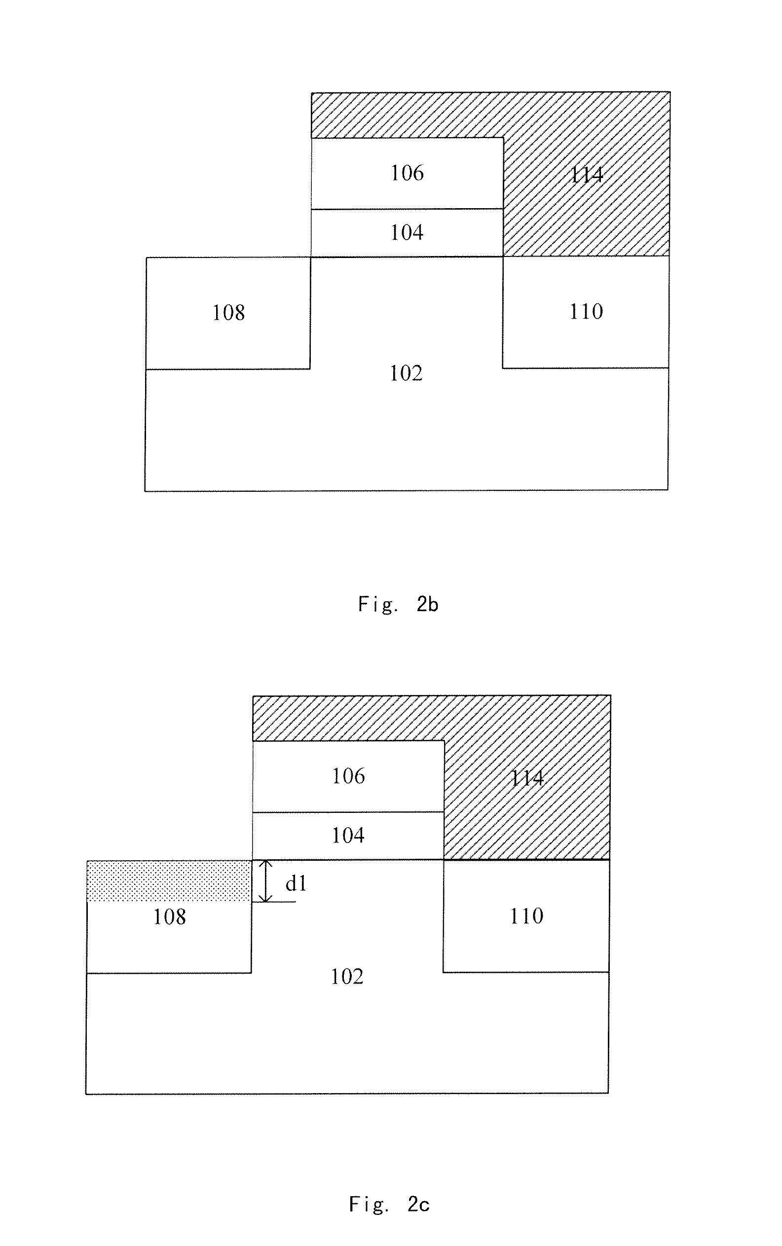
[0044]FIG. 6 shows the transistor according to the third embodiment of the present invention. The transistor 300 shown in FIG. 6 is different from the transistor 100 shown in FIG. 1 in that the source region 108 comprises a set of two dislocations which are adjacent to the channel region 112 and arranged in the direction perpendicular to the top surface of the semiconductor substrate 102.

[0045]Accordingly, as compared with the method for forming the transistor 100 in the first embodiment, the method for forming the transistor 300 according to the present embodiment further comprises performing a second ion implantation with a second implantation depth of d2 to the source region 108 after the annealing step of the method of the first embodiment, with the second implantation depth d2 being smaller than the first implantation depth d1, as shown in FIG. 7. An annealing is performed after the second ion implantation and the device shown in FIG. 6 is obtained. The impl...


PUM


Abstract

The present invention relates to a transistor and the method for forming the same. The transistor of the present invention comprises a semiconductor substrate; a gate dielectric layer formed on the semiconductor substrate; a gate formed on the gate dielectric layer; and a source region and a drain region located in the semiconductor substrate and on respective sides of the gate, wherein only the source region comprises at least one dislocation. The method for forming a transistor according to the present invention comprises forming a mask layer on a semiconductor substrate on which a gate has been formed so that the mask layer covers the gate and the semiconductor substrate; patterning the mask layer to only expose at least a portion of a source region; performing a first ion implantation to the exposed portion of the source region; and annealing the semiconductor substrate so as to form a dislocation in the exposed portion of the source region.

Description

CLAIM OF PRIORITY[0001]This application claims priority under 35 U.S.C. §§120 and 365(c) as a continuation application of prior International Application No. PCT / CN2011 / 000280, filed Feb. 23, 2011, and which was not published in English under PCT Article 21(2). The PCT / CN2011 / 000280 application in turn claims priority to Chinese Application No. CN 201010532061.4, filed on Oct. 29, 2010. The disclosures of the prior international application and Chinese application are incorporated herein by reference.FIELD OF THE INVENTION[0002]The present invention relates to the field of semiconductor device manufacturing, and particularly, to a transistor and a method for forming the same.BACKGROUND OF THE INVENTION[0003]Typically, integrated circuits comprise a combination of N-type Metal Oxide Semiconductor (NMOS) and P-type Metal Oxide Semiconductor (PMOS) transistors formed on a substrate. The performance of an integrated circuit is directly related to the performance of transistors which it ...

Claims


Application Information

Patent Timeline
IPC IPC(8): H01L29/78H01L21/336
CPCH01L21/26506H01L29/04H01L29/66659H01L29/78H01L29/7848H01L21/823807H01L21/823814H01L29/32H01L21/26513
Inventor YIN, HAIZHOULUO, ZHIJONGZHU, HUILONG
Owner INST OF MICROELECTRONICS CHINESE ACAD OF SCI
Why Eureka
Try Eureka