
Highly Uniform Group III Nitride Epitaxial Layers on 100 Millimeter Diameter Silicon Carbide Substrates

Active Publication Date: 2008-12-11
WOLFSPEED INC
View PDF17 Cites 1 Cited by
  • Summary
  • Abstract
  • Description
  • Claims
  • Application Information

AI Technical Summary

Benefits of technology

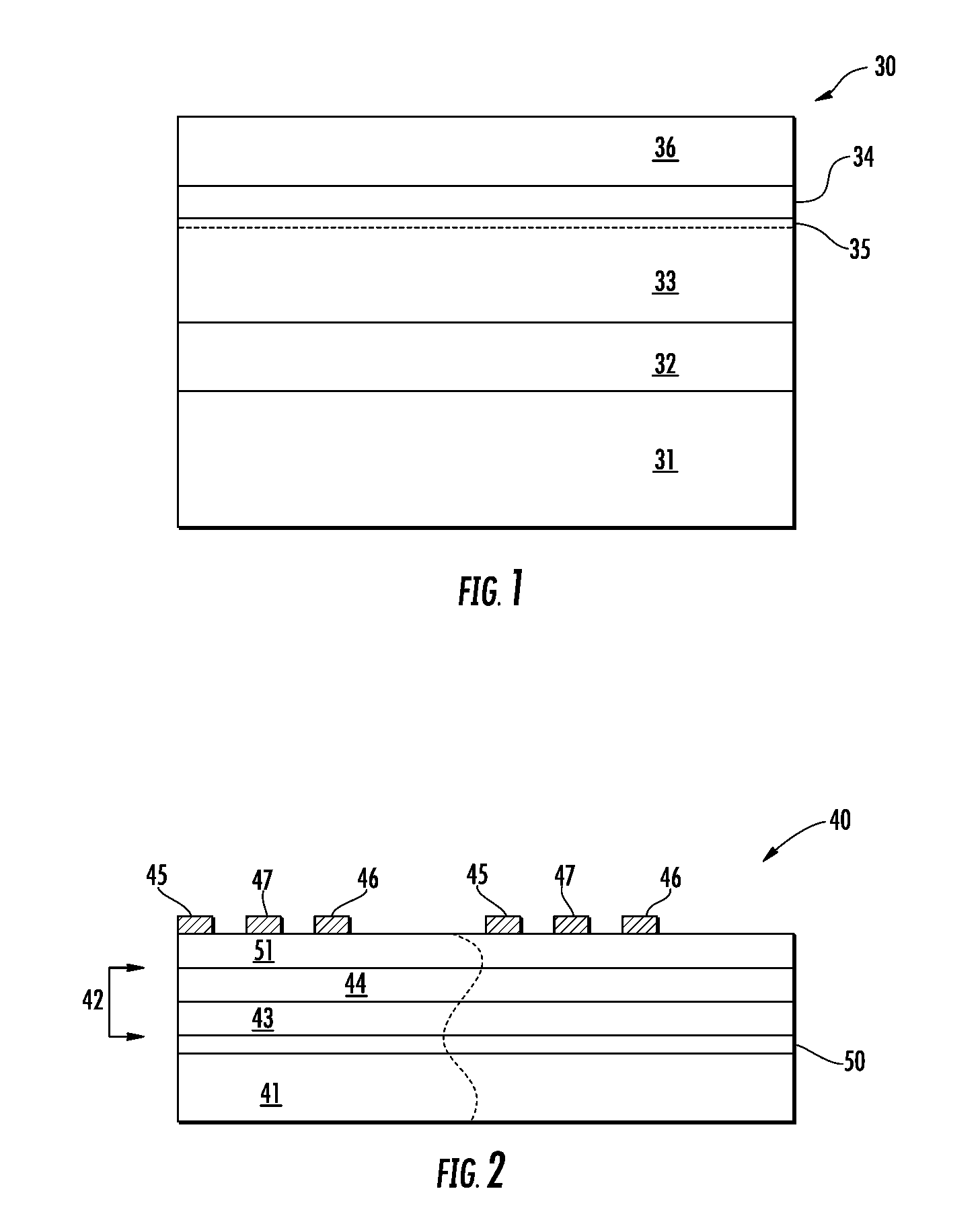
[0014]In one aspect, the invention is a semiconductor precursor structure comprising a silicon carbide single crystal substrate at least 100 millimeters in diameter, a Group III nitride nucleation layer on the substrate, a first Group III nitride epitaxial layer on the nucleation layer, a second Group III nitride epitaxial layer on the first Group III nitride epitaxial layer and having a composition sufficiently different from the composition of the first layer to generate a two-dimensional electron gas at the interface between the first and second layers. A third Group III nitride epitaxial layer may be on the second layer for increasing the electron mobility in the two-dimensional electron gas. The precursor structure has a sheet resistivity standard deviation of no more than about one percent (1%) across the 100 millimeter structure and the precursor structure also has a mobility standard deviation across the 100 millimeter structure of no more than about one percent.

Problems solved by technology

Nevertheless, gallium arsenide has a relatively small bandgap (1.42 eV) and a relatively small breakdown voltage which limits the higher power, higher frequency applications with which makes gallium arsenide less suitable, or in some cases unsuitable, for higher power, higher frequency applications.
The lack of quality or uniformity in the materials, or in material structures that form devices or device precursors, reduces the yield and limits the sizes of resulting devices that are potentially available from the material systems.
To date, higher quality Group III nitride structures are available on two inch and three inch wafers, but these are less advantageous for larger power devices.
Additionally, because the edge of every wafer, regardless of size, typically requires about an 8 mm loss, edge losses are proportionally high for smaller wafers.
Processing costs, however, are typically similar regardless of the size of a wafer so that smaller wafers increase manufacturing costs per device of a given size.

Method used


Image

  • Highly Uniform Group III Nitride Epitaxial Layers on 100 Millimeter Diameter Silicon Carbide Substrates
  • Highly Uniform Group III Nitride Epitaxial Layers on 100 Millimeter Diameter Silicon Carbide Substrates
  • Highly Uniform Group III Nitride Epitaxial Layers on 100 Millimeter Diameter Silicon Carbide Substrates

Examples


Embodiment Construction

[0034]In one aspect, the present invention is a highly uniform and robust quality aluminum gallium nitride high electron mobility transistor (HEMT) structure formed from 100 millimeter (i.e., slightly smaller than four inch) diameter silicon carbide substrates.

[0035]In another aspect, the invention is the highly uniform 100 millimeter diameter wafer precursor upon which individual HEMTs are formed.

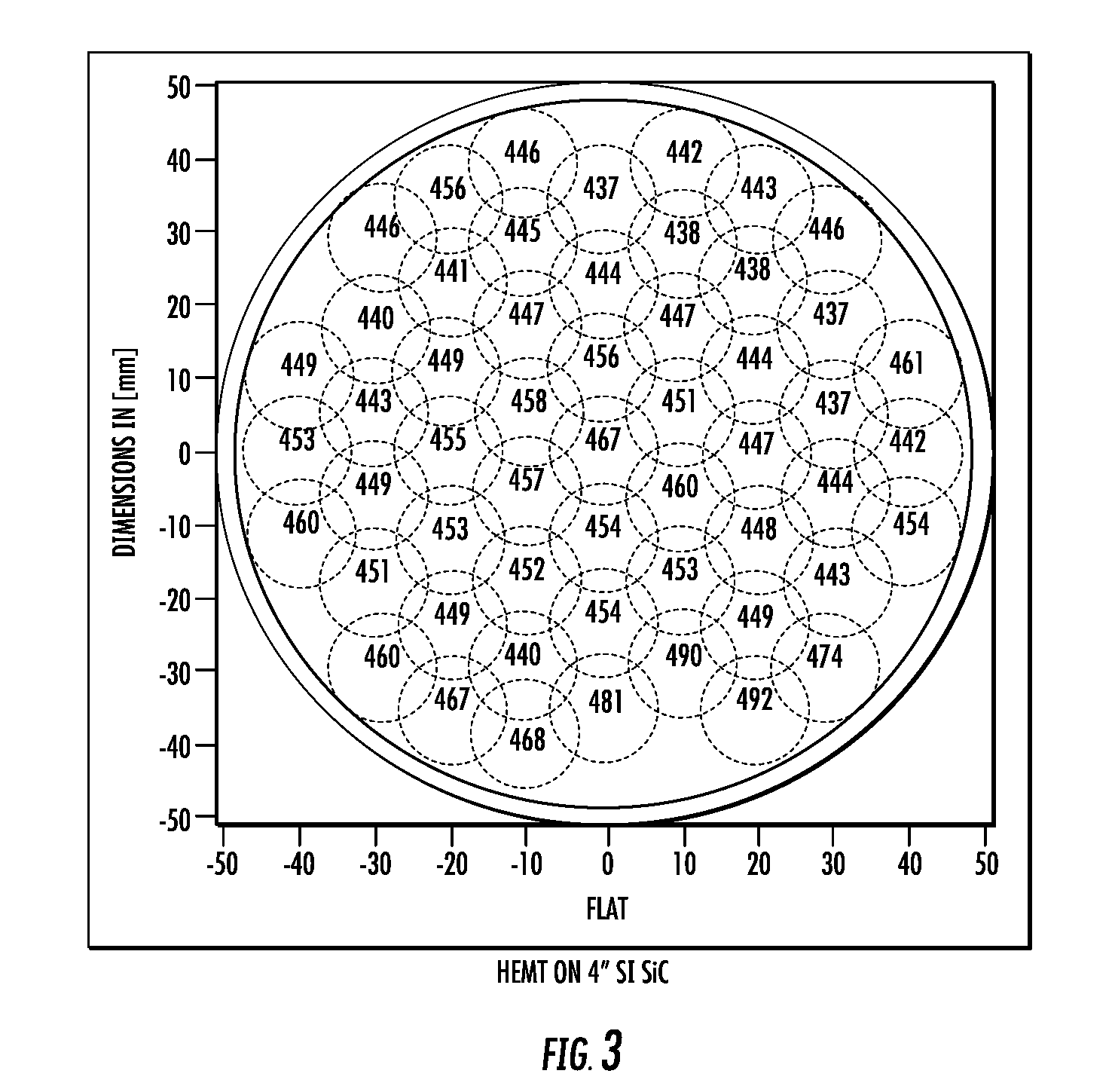
[0036]In another aspect, the invention is a plurality of HEMTs on a highly uniform 100 millimeter diameter substrate structure.

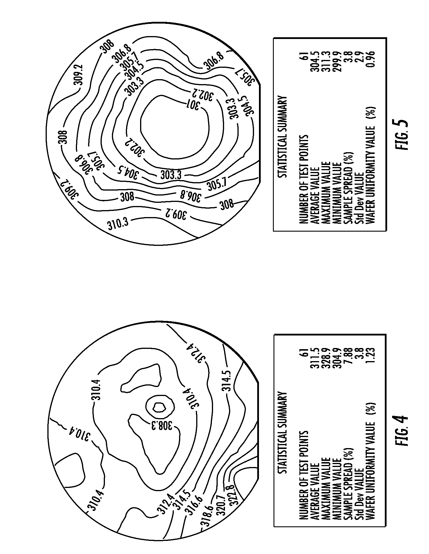
[0037]HEMT precursors according to the invention are formed from epitaxial growth processes that produce heterostructure and related layers that are highly uniform in their physical, chemical and electronic properties. The observed uniformity differences are typically one percent or less, with electron mobility at room temperature greater than 2000 cm2 / V-s. These growth techniques result in extremely smooth epitaxial layers, are repeatable, and show resistance impr...


PUM


Abstract

A semiconductor structure is disclosed that includes a silicon carbide wafer having a diameter of at least 100 mm with a Group III nitride heterostructure on the wafer that exhibits high uniformity in a number of characteristics. These include: a standard deviation in sheet resistivity across the wafer less than three percent; a standard deviation in electron mobility across the wafer of less than 1 percent; a standard deviation in carrier density across the wafer of no more than about 3.3 percent; and a standard deviation in conductivity across the wafer of about 2.5 percent.

Description

RELATED APPLICATIONS[0001]This is a divisional application of Ser. No. 11 / 149,664 filed Jun. 10, 2005.[0002]This invention was developed under Government Contract Nos. N0014-02-C-0321 and N00014-02-C-0306. The Government may have certain rights in this invention.BACKGROUND[0003]The present invention relates to the use of semiconductor materials for high frequency high-power applications and in particular relates to the use of Group III nitride materials for high electron mobility transistors (HEMTs), and most particularly to improvements in these material systems that lead to corresponding improvements in the electronic performance of the transistors.[0004]A HEMT is a solid-state transistor that offers advantages for signal amplification in applications such as (but not limited to) radar, cellular telephone communications, satellite communications and other microwave circuit applications.[0005]A HEMT behaves much like a conventional Field Effect Transistor (FET). A conducting channe...

Claims


Application Information

Patent Timeline
IPC IPC(8): C30B23/02
CPCC30B29/36C30B29/403C30B29/406H01L29/2003H01L29/7787
Inventor SAXLER, ADAM WILLIAMHUTCHINS, EDWARD LLOYD
Owner WOLFSPEED INC
Learn More