Flat Panel Display Structure and Manufacturing Method Thereof

a technology of display structure and flat panel, which is applied in the field of flat panel display structure, can solve the problems of weakening and weakening the structural strength of films simply placed in the backlight module, and affecting the performance of backlight modules, so as to enhance the strength of the whole structure, and prevent deformation of components

Inactive Publication Date: 2012-05-03
AU OPTRONICS CORP
View PDF9 Cites 50 Cited by
  • Summary
  • Abstract
  • Description
  • Claims
  • Application Information

AI Technical Summary

Benefits of technology

[0007]One object of the present invention is to provide a flat panel display structure. Comparing to the prior art, the flat panel display structure of the present invention can prevent deformation of components such as optical films and display panel and can enhance the strength of the whole structure.
[0008]Another object of the present invention is to provide a manufacturing method of the above-mentioned flat panel display structure. Comparing to the prior art, the manufacturing method of the present invention can prevent deformation of components such as optical films and display panel and can also simplify the process of assembling components.
[0009]The flat panel display structure of the present invention includes a light guide plate, an optical film, a first glue layer, a display panel, a second glue layer, and a light module emitting light toward the light guide plate. The light guide plate is made of optical glass. The optical film is disposed on the light guide plate and attached thereto by the first glue layer. The display panel includes a light incident surface and a display surface, wherein the light incident surface faces the optical film and the central portion of the display surface has an active area. The second glue layer attaches the optical film to the display panel and covers the light incident surface including the projection of the active area thereon. The reflective indices of the first glue layer and the second glue layer are both less than or equal to the reflective indices of light guide plate and the optical film. The flat panel display structure of the present invention utilizes the structure of the display panel, the optical film, and the light guide plate attached to one another to prevent deformation of components such as optical film and display panel and enhances the strength of the whole structure.
[0010]The manufacturing method of the flat display structure of the present invention includes the following steps: disposing and attaching a first glue layer between optical film and a light guide plate made of an optical glass; disposing and attaching a second glue layer between the optical film and a display panel to allow a light incident surface of the display panel to face the optical film, the second glue layer covering the light incident surface including the projection of an active area; disposing a light module emitting light toward the light guide plate. The reflective indices of the first glue layer and the second glue layer are both smaller than or equal to the reflective indices of the light guide plate and the optical film, and the active area is located on a central portion of the display surface opposite to the light incident surface. The manufacturing method of the present invention, on the one hand, prevents deformation of components such as optical film and display panel by attaching the display panel, the optical film, and the light guide plate to one another; on the other hand, it simplifies the process of assembling components.

Problems solved by technology

However, the optical films simply placed in the backlight module are susceptible to deformation and such deformation will be more obvious in large-scale products.
Also, as the liquid crystal display keeps getting thinner and thinner, its structural strength becomes weaker and weaker.

Method used


Image

  • Flat Panel Display Structure and Manufacturing Method Thereof
  • Flat Panel Display Structure and Manufacturing Method Thereof
  • Flat Panel Display Structure and Manufacturing Method Thereof

Examples


first embodiment

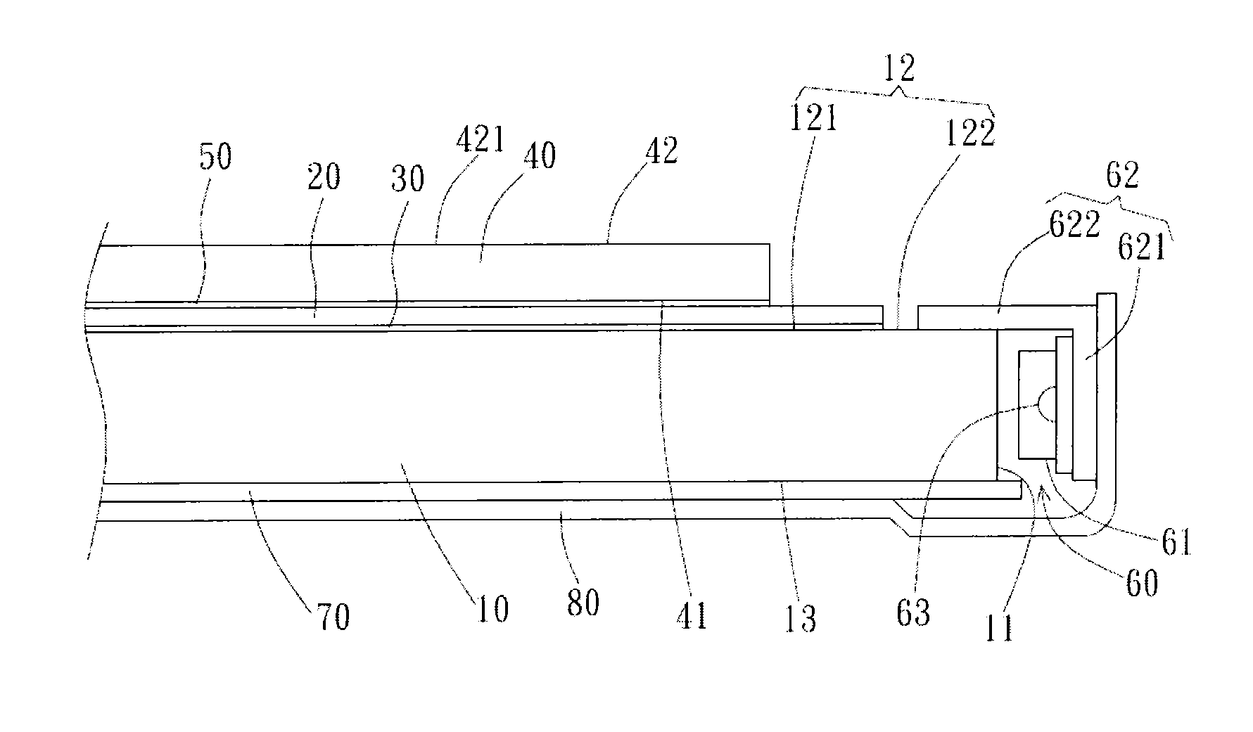
[0033]FIG. 1 is a cross-sectional view of the flat panel display structure. As shown in FIG. 1, the flat panel display structure includes a light guide plate 10, an optical film 20, a first glue layer 30, a display panel 40, a second glue layer 50, a light module 60, a reflector 70, and a back plate 80. The light guide plate 10 is an optical glass and the material can be soda glass, silica glass, ultra clear glass, or other types of optical glass. The light guide plate 10 includes a light incident side 11, a light emitting surface 12, and a bottom surface 13, the light emitting surface 12 and the bottom surface 13 are two opposite surfaces connected to an edge of the light incident side 11, respectively. The light emitting surface 12 faces the optical film 20. The optical film 20 is disposed on the light guide plate 10 and attached onto the light guide plate 10 by the first glue layer 30. In a preferred embodiment, the optical film 20 is a multilayer composite film; however, in othe...

second embodiment

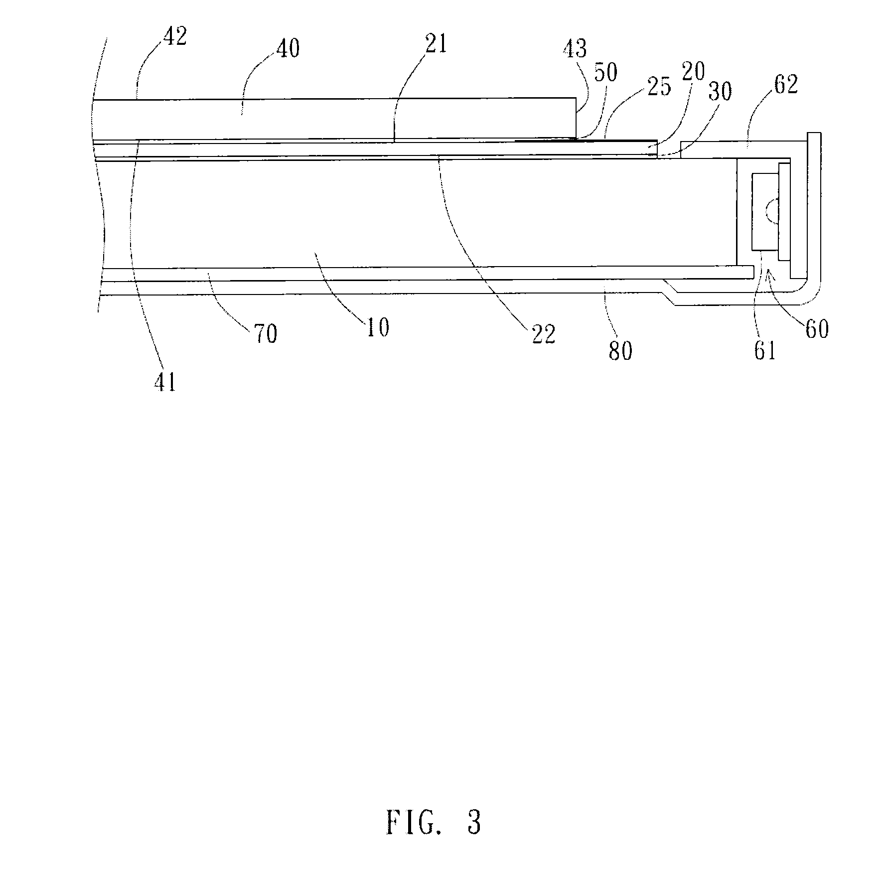
[0036]FIG. 3 is a schematic view of the flat panel display structure. As shown in FIG. 3, in this embodiment, the optical film 20 includes an upper surface 21 and a lower surface 22 opposite to the upper surface 21, wherein a light shielding layer 25 is formed on the periphery of the upper surface 21 facing the display 40 to prevent glare from occurring at the periphery of the display panel 40 to affect the visual effect. The light shielding layer 25 extends inward to cross the projection of the display panel 40 on the optical film 20. That is, the light shielding layer 25 extends to cross the boundary of the side edge 43 of the display panel 40 and the light incident surface 41. The light shielding layer 25 is preferably made by ink printing and the second glue layer 50 covers at least a portion of the light shielding layer 25. In this embodiment, the second glue layer 50 covers a portion of the light shielding layer 25 that faces the light incident surface 41. In other embodiments...

third embodiment

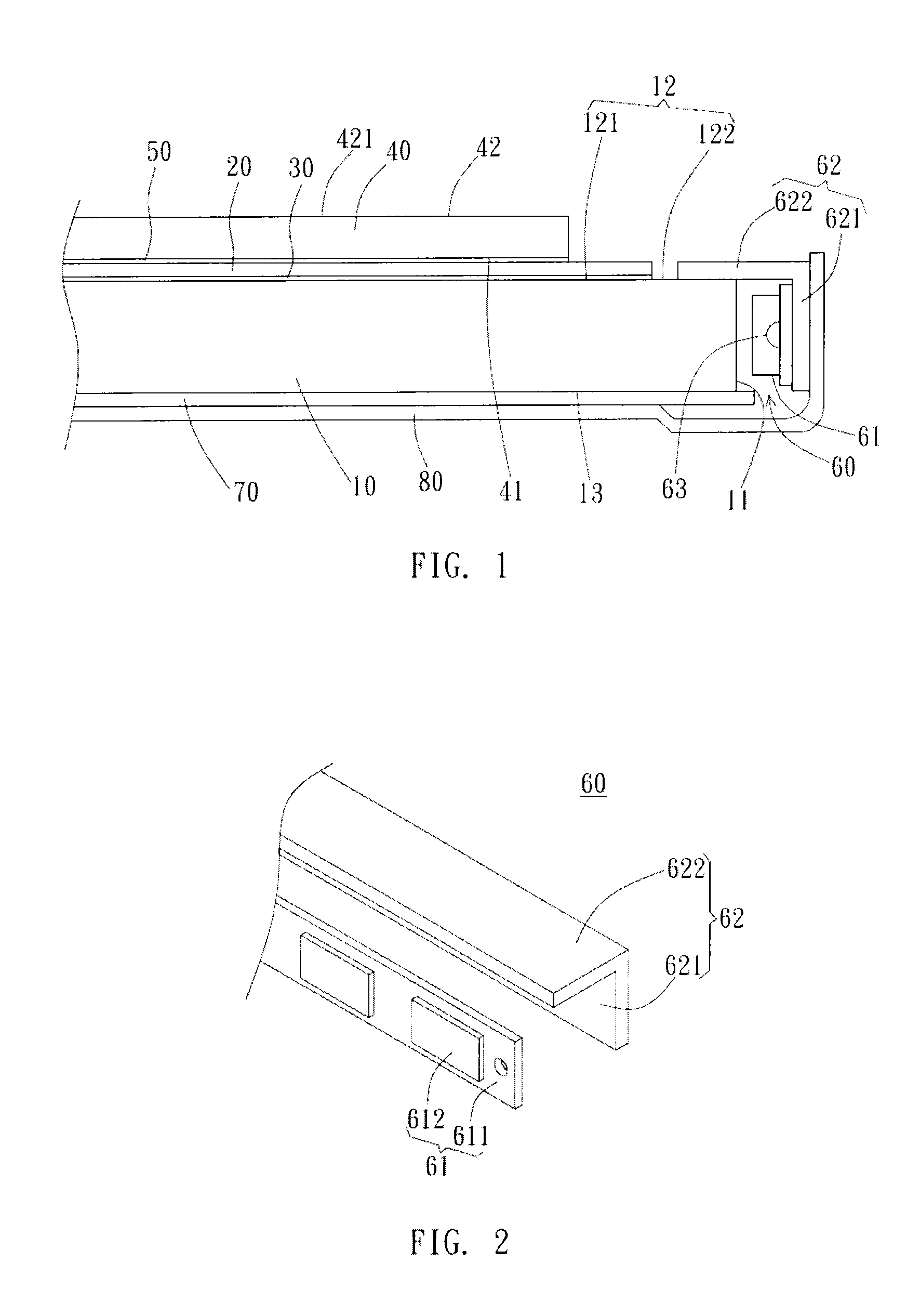
[0037]FIG. 4 is a schematic view of the flat panel display structure. As shown in FIG. 4, the back plate 80 includes a bottom plate 81 and a sidewall 82 connected at an angle. The light guide plate 10 is disposed on the bottom plate 81 and the sidewall 82 has an inner surface 821 and an outer surface 822. The light emitting unit 61 is disposed on the inner surface 821 that faces the light guide plate 10 and the first reflective portion 621 of the reflective cover 62 is attached to the outer surface 822. In this embodiment, the double-sided tape is used to attach the light module 60 to the light guide plate 10 as well as the light module 60 to the back plate 80; however, in other embodiments, the connection or attachment may be achieved by other types of adhesive materials.


PUM

PropertyMeasurementUnit
refractive indicesaaaaaaaaaa
refractive indexaaaaaaaaaa

Abstract

A flat panel display structure and a manufacturing method thereof are provided. The flat panel display structure includes a light guide plate made of optical glass, an optical film disposed on the light guide plate and glued thereon through a first glue layer, a display panel having a light incident surface facing the optical film and a display surface with an active area located at the central portion thereof, a second glue layer gluing the optical film and the display panel so as to cover the light incident surface including the projection of the display area thereon, and a light module emitting lights toward the light guide plate. The refractive indices of the first glue layer and the second glue layer are smaller than or equal to that of the light guide plate and the optical film.

Description

BACKGROUND OF THE INVENTION[0001]1. Field of the Invention[0002]The present invention relates to a flat panel display structure and a manufacturing method thereof. Particularly, the present invention relates a to a flat panel display structure of a display panel, an optical film, and a light guide plate attached to one another.[0003]2. Description of the Prior Art[0004]Besides the display panel, the most important unit in the liquid crystal display is the backlight module. The backlight module is used for providing an outer light source to achieve the display function because the liquid crystal molecular itself can not emit light. The backlight module disposed behind the liquid crystal display panel is mainly composed of a light guide plate and a light emitting component. Light emitted from the light emitting component is transmitted through the light guide plate and projects uniformly to the liquid crystal display panel to form the display light source.[0005]In addition, in order t...

Claims


Application Information

Patent Timeline
Patent Type & Authority Applications(United States)
IPC IPC(8): F21V7/00B32B37/14B32B38/04F21V8/00B32B37/12
CPCB32B37/12B32B2037/1223B32B2457/20B32B2457/202G02B6/0031G02B6/0088G02B6/009Y10T156/1056
Inventor LAI, CHING-KUNCHEN, CHING-CHUANHONG, HONG-JYE
Owner AU OPTRONICS CORP
Why Eureka
Try Eureka