Method for manufacturing semiconductor device

a semiconductor and manufacturing method technology, applied in the direction of semiconductor devices, electrical appliances, transistors, etc., can solve the problems of increasing leakage current and scaling down the gate of the mos transistor, and achieve the effect of increasing stress, enhancing mobility of carriers, and increasing stress

Active Publication Date: 2012-05-03
SAMSUNG ELECTRONICS CO LTD
View PDF3 Cites 2 Cited by
  • Summary
  • Abstract
  • Description
  • Claims
  • Application Information

AI Technical Summary

Benefits of technology

[0011]As described above, the mobility of carriers can be enhanced by increasing stress applied to a channel. In addition, the mobility of carriers can be more effectively enhanced by inducing

Problems solved by technology
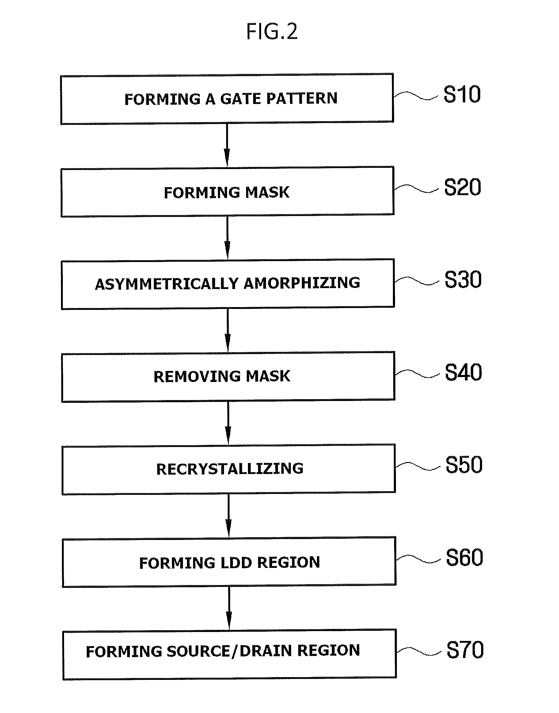
As an integration degree of the semiconductor device is increased, scaling down a gate of the MOS transistor is becoming a major challenge.
The stress memoriza

Method used


Image

  • Method for manufacturing semiconductor device
  • Method for manufacturing semiconductor device
  • Method for manufacturing semiconductor device

Examples


Embodiment Construction

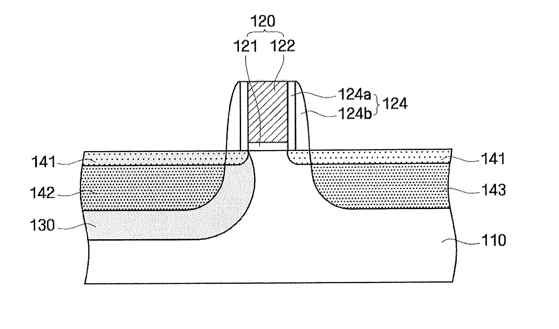
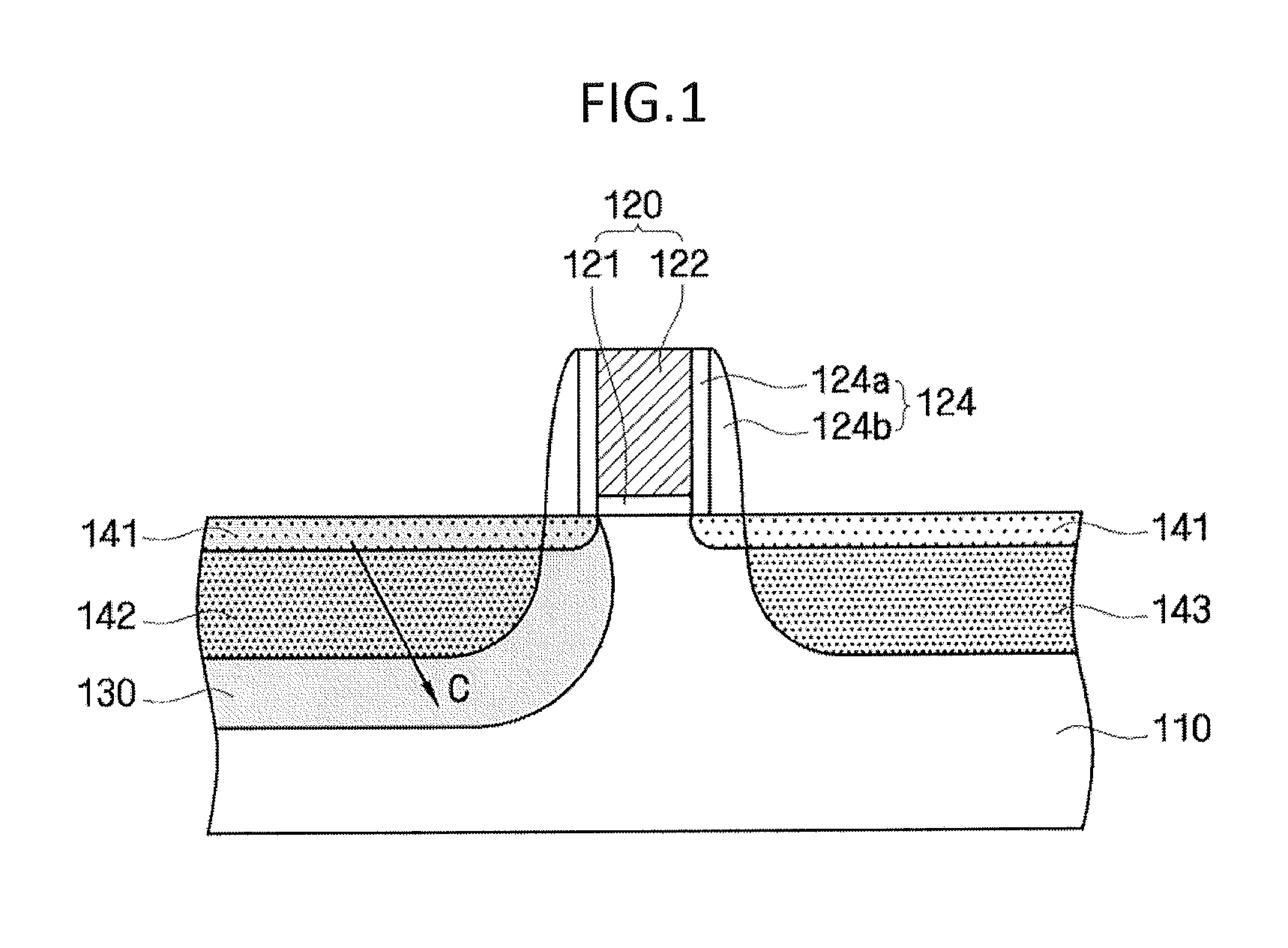
[0016]Advantages and features of the present invention and methods of accomplishing the same may be understood more readily by reference to the following detailed description of exemplary embodiments and the accompanying drawings. The present invention may, however, be embodied in many different forms and should not be construed as being limited to the embodiments set forth herein. Rather, these embodiments are provided so that this disclosure will be thorough and complete and will fully convey the concept of the invention to those skilled in the art, and the present invention will only be defined by the appended claims. In the drawings, the thickness of layers and regions are exaggerated for clarity.

[0017]It will be understood that when an element or layer is referred to as being “on” or “connected to” another element or layer, it can be directly on or connected to the other element or layer, or intervening elements or layers may be present. In contrast, when an element is referred...


PUM


Abstract

A semiconductor device is formed with a gate pattern formed on a substrate, and a recrystallized region having a stacking fault defect in the substrate at one side of the gate pattern. The semiconductor device can have a reduced leakage current and improved channel conductivity.

Description

CROSS-REFERENCE TO RELATED APPLICATION[0001]This application claims priority from Korean Patent Application No. 10-2010-0106302 filed on Oct. 28, 2010 in the Korean Intellectual Property Office, and all the benefits accruing therefrom under 35 U.S.C. 119; the entire contents of this priority application are herein incorporated by reference.BACKGROUND OF THE INVENTION[0002]1. Field of the Invention[0003]The present invention relates to a semiconductor device and a method for manufacturing the same, and more particularly to a semiconductor device having a reduced leakage current and improved channel conductivity, and a method for manufacturing the semiconductor device.[0004]2. Description of the Related Art[0005]Research is under way to increase the operation speed and packing density of semiconductor devices. A semiconductor increases discrete devices such as a metal oxide semiconductor (MOS) transistor. As an integration degree of the semiconductor device is increased, scaling down ...

Claims


Application Information

Patent Timeline
IPC IPC(8): H01L21/336
CPCH01L21/26506H01L21/26586H01L29/6659H01L29/66659H01L21/26513H01L29/7847H01L21/2658H01L21/2654H01L21/26546H01L29/7835H01L29/1025
Inventor LIM, KWAN-YONGKOH, CHUNG-GEUNKANG, SANG-BOMKWON, UI-HUILEE, HYUN-JUNGKWON, TAE-OUKKIM, SEOK-HOON
Owner SAMSUNG ELECTRONICS CO LTD
Why Eureka
Try Eureka