

Organic thin-film transistor, and process for production thereof
a thin-film transistor and organic technology, applied in the direction of thermoelectric device junction materials, semiconductor devices, electrical apparatus, etc., can solve the problems of current flow drop, achieve large current, and increase the efficiency of hole-electron injection
- Summary
- Abstract
- Description
- Claims
- Application Information
AI Technical Summary
Benefits of technology
Problems solved by technology
Method used
Image

Examples
embodiment 1
Arrangement of Organic Thin-Film Transistor 100
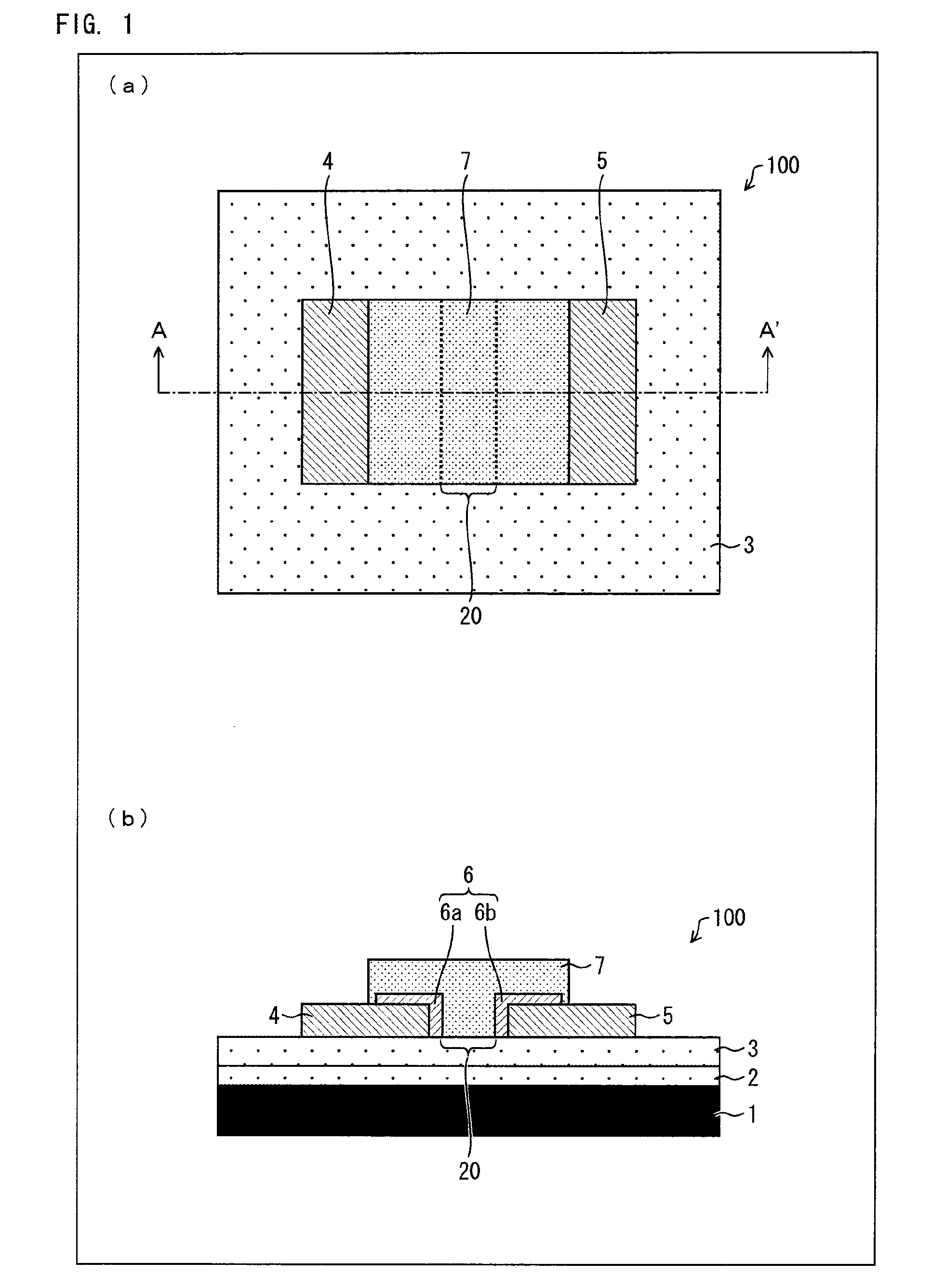
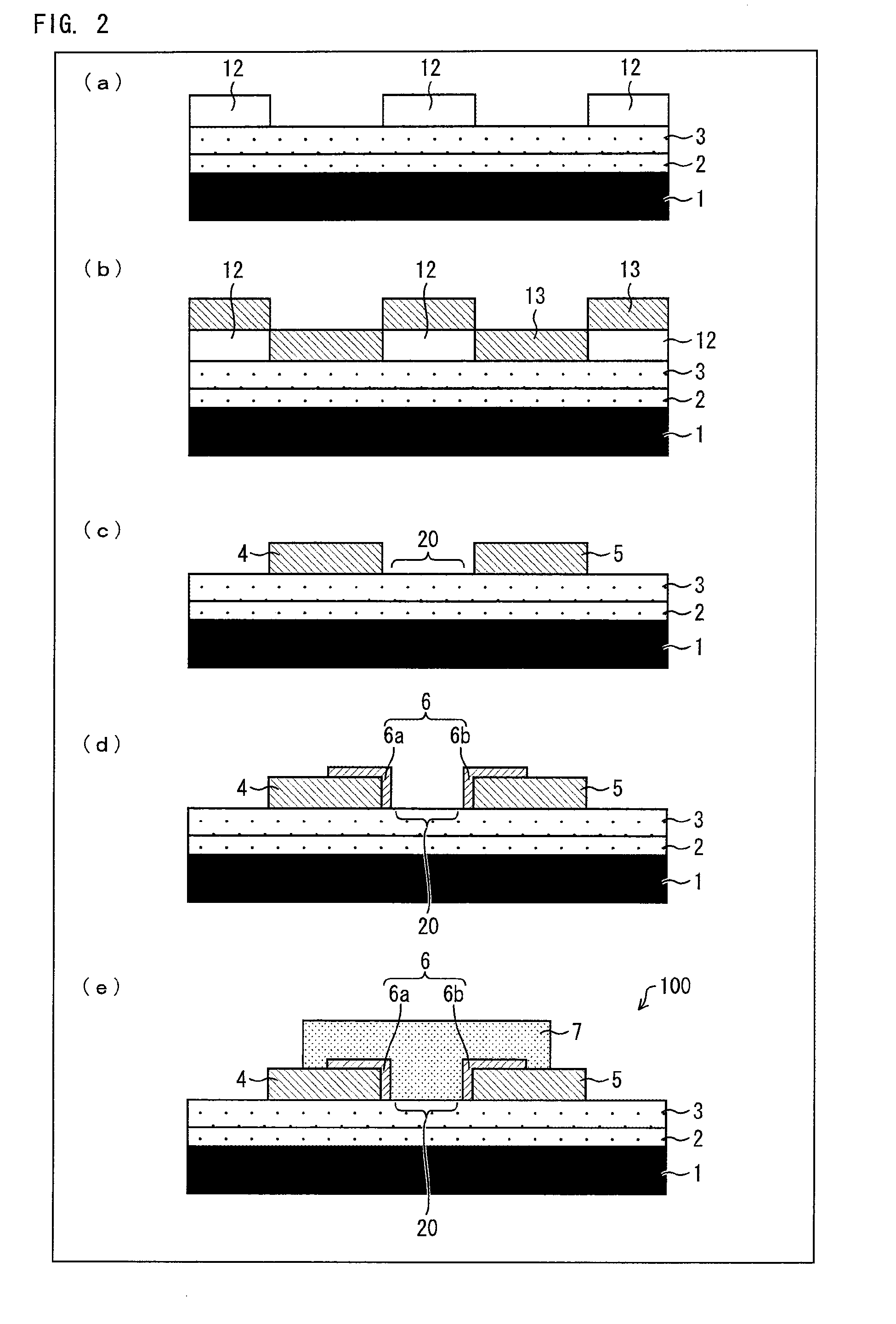
[0051]The following describes an arrangement of an organic thin-film transistor 100 of the present embodiment, with reference to FIG. 1. (a) of FIG. 1 is a view illustrating a top surface of the organic thin-film transistor 100. (b) of FIG. 1 is a cross-sectional view illustrating a cross-section taken along the line A-A′ in (a) of FIG. 1.
[0052]As illustrated in (b) of FIG. 1, the organic thin-film transistor 100 is a transistor of a bottom contact-type. The organic thin-film transistor 100 includes a substrate 1, a gate electrode 2, a gate insulating layer 3, a source electrode 4, a drain electrode 5, organic molecular layers 6, and an organic semiconductor layer 7. Specifically, the gate electrode 2 is formed on the substrate 1. The gate insulating layer 3 is formed on the gate electrode 2. The source electrode 4 and the drain electrode 5, spaced from each other, are provided on the gate insulating layer 3. A part of a top surface of ...
embodiment 2
Arrangement of Organic Thin-Film Transistor 200
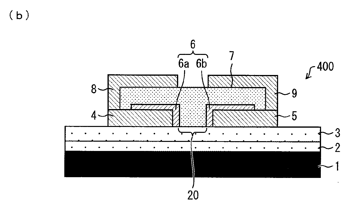
[0077]An organic thin-film transistor 200 of the present embodiment is characterized by including a second source electrode 8 and a second drain electrode 9. The following concretely describes this, with reference to FIG. 5. (a) of FIG. 5 illustrates a top surface of the organic thin-film transistor 200. (b) of FIG. 5 is a cross-sectional view taken along the line A-A′ in (a) of FIG. 5.
[0078]As illustrated in (b) of FIG. 5, the organic thin-film transistor 200 is a bottom contact-type transistor. The organic thin-film transistor 200 includes a substrate 1, a gate electrode 2, a gate insulating layer 3, a source electrode 4, a drain electrode 5, organic molecular layers 6, an organic semiconductor layer 7, the second source electrode 8, and the second drain electrode 9. Specifically, the gate electrode 2 is formed on the substrate 1. The gate insulating layer 3 is formed on the gate electrode 2. The source electrode 4 and the drain elect...
embodiment 3
[0087]As is the case with Embodiment 2, an organic thin-film transistor 300 of the present embodiment includes a second source electrode 8 and a second drain electrode 9. However, the organic semiconductor layer 7 is provided so as to have a contact with a part of a top surface of each of the source electrode 4 and the drain electrode 5. The following concretely describes this, with reference to FIG. 9. (a) of FIG. 9 illustrates a top surface of the organic thin-film transistor 300. (b) of FIG. 9 is a cross-sectional view taken along the line A-A′ in (a) of FIG. 9.
[0088]As illustrated in (b) of FIG. 9, the organic thin-film transistor 300 is a bottom contact-type transistor. The organic thin-film transistor 300 includes a substrate 1, a gate electrode 2, a gate insulating layer 3, a source electrode 4, a drain electrode 5, an organic molecular layer 6, an organic semiconductor layer 7, the second source electrode 8, and the second drain electrode 9. Specifically, the gate electrode ...
PUM
 Abstract
Description
Claims
Application Information