Virtual Photo-Mask Critical-Dimension Measurement

a photo-mask and critical-dimension technology, applied in the field of virtual photo-mask critical-dimension measurement, can solve the problems of wide new class of problems in photo-mask inspection and qualification, unclear what impact this defect will have on the final pattern of the photo-mask, and errors may be introduced

Active Publication Date: 2012-05-31
KLA TENCOR TECH CORP
View PDF2 Cites 19 Cited by
  • Summary
  • Abstract
  • Description
  • Claims
  • Application Information

AI Technical Summary

Benefits of technology

[0017]In the constrained inverse optical calculation, the image may be at an image plane of a model of the optical path and the mask pattern may be at an object plane of the model of the optical path. Furthermore, by constraining the inverse optical calculation, a convergence time of the inverse optical calculation may be faster than that of an unconstrained inverse optical calculation.

Problems solved by technology

Unfortunately, as dimensions in integrated circuits steadily become a smaller fraction of the wavelength of the light used to expose images of the photo-mask onto the wafer, the structures in or on the ideal photo-mask (which corresponds to a ‘target mask pattern’) and / or the physical structures in or on the actual photo-mask (which corresponds to a fabricated ‘mask pattern’) bear less and less resemblance to the desired or target pattern at the wafer.
From a photo-mask or reticle manufacturing standpoint, the increasing dissimilarity between the photo-mask and the corresponding wafer patterns creates a broad new class of problems in photo-mask inspection and qualification.
For example, if a defect in a photo-mask is detected, it is often unclear what impact this defect will have on the final pattern in the photoresist.
However, since the optical inspection images of the photo-mask may not be an accurate representation of the actual photo-mask, errors may be introduced when simulating wafer patterns, and thus, when trying to identify or classify defects.
This may further complicate photo-mask inspection and qualification.
However, measuring a CD-SEM image can be time consuming and complicated.
In particular, the electron beam in an SEM often leads to charging of the photo-mask, which can attract dirt or contamination.
Furthermore, subsequent cleaning of the photo-mask may produce additional defects in the photo-mask that are not included in the CD-SEM image and, thus, will not be included in the simulations.
Therefore, even though a CD-SEM image can provide a more accurate representation of the original physical photo-mask, errors may still be introduced when simulating wafer patterns, and thus, when trying to identify or classify defects.

Method used


Image

  • Virtual Photo-Mask Critical-Dimension Measurement
  • Virtual Photo-Mask Critical-Dimension Measurement
  • Virtual Photo-Mask Critical-Dimension Measurement

Examples


Embodiment Construction

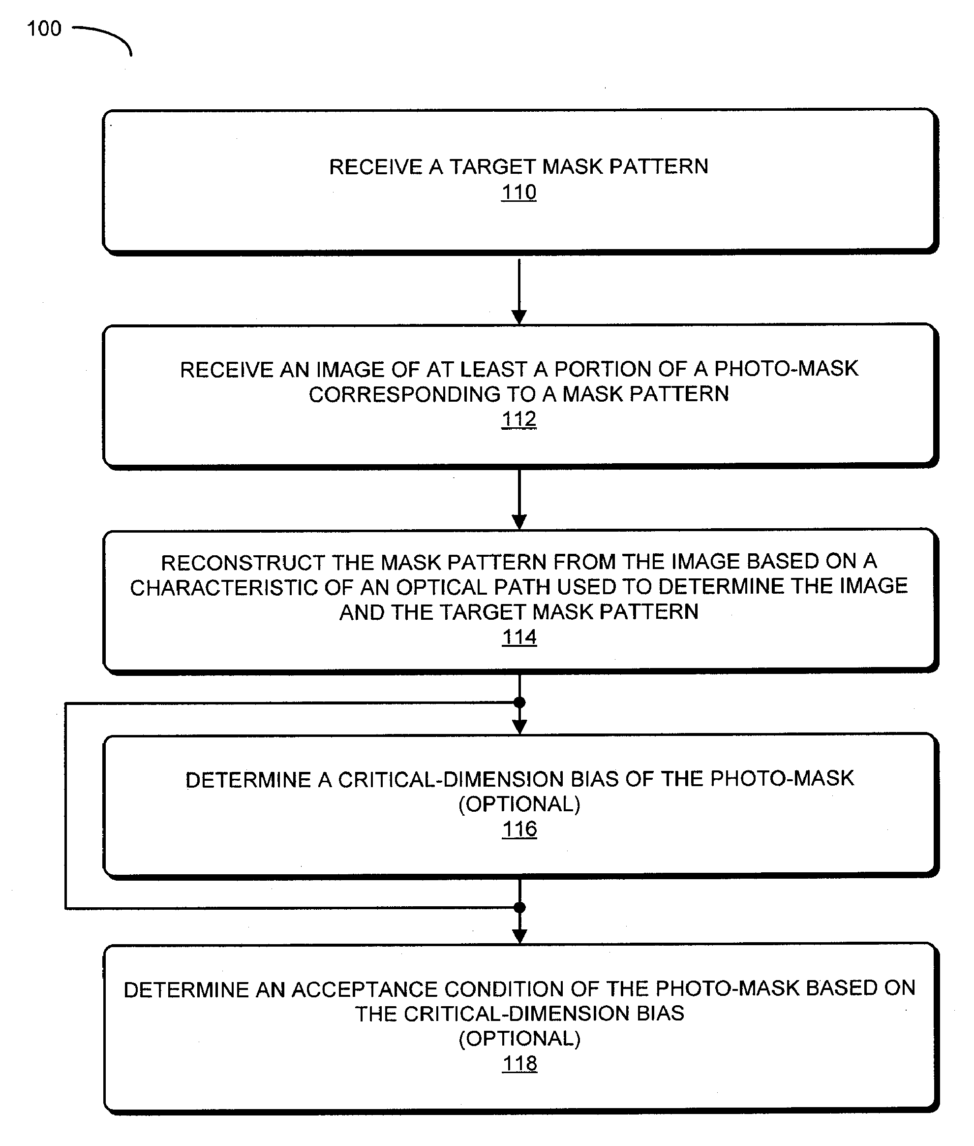
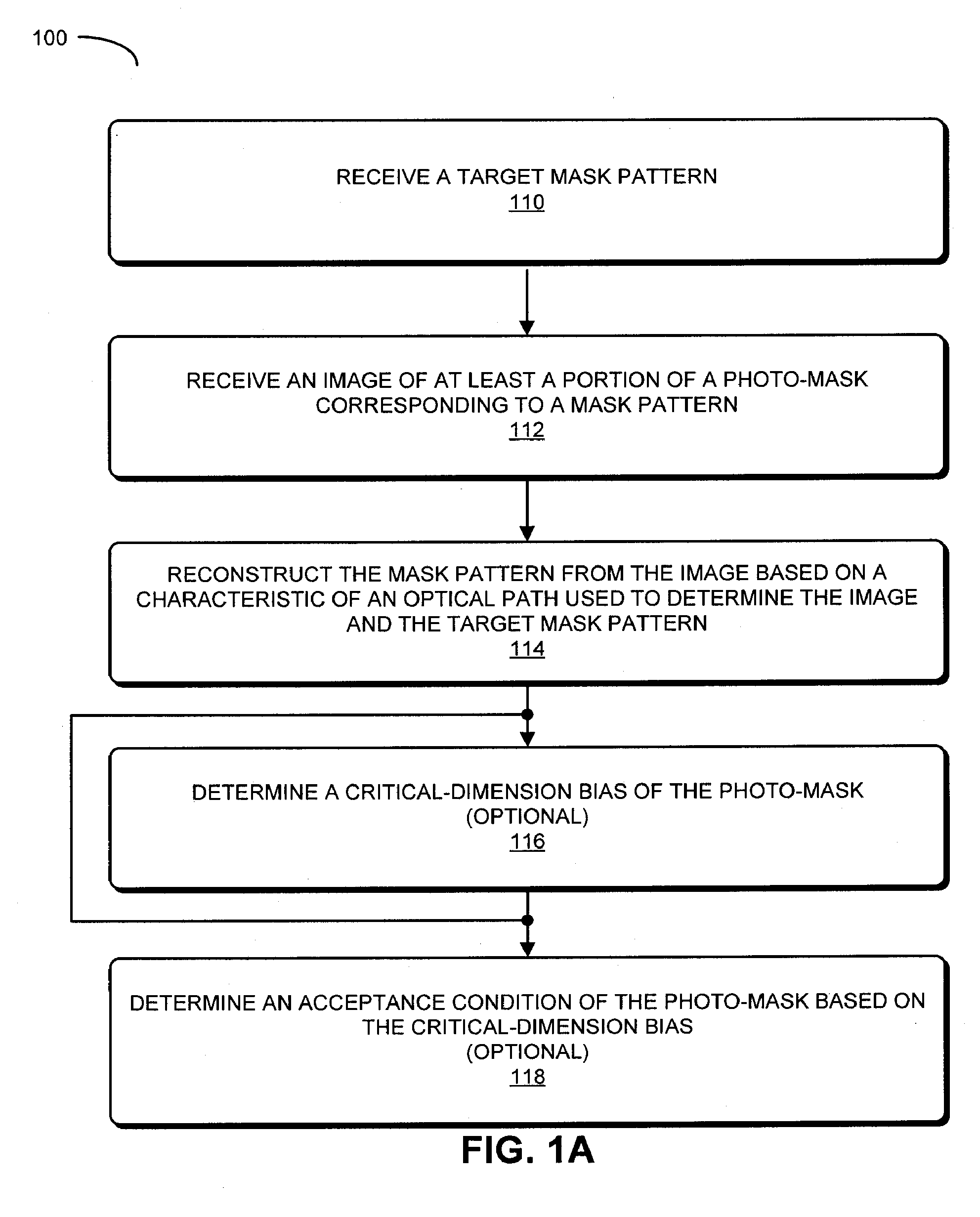
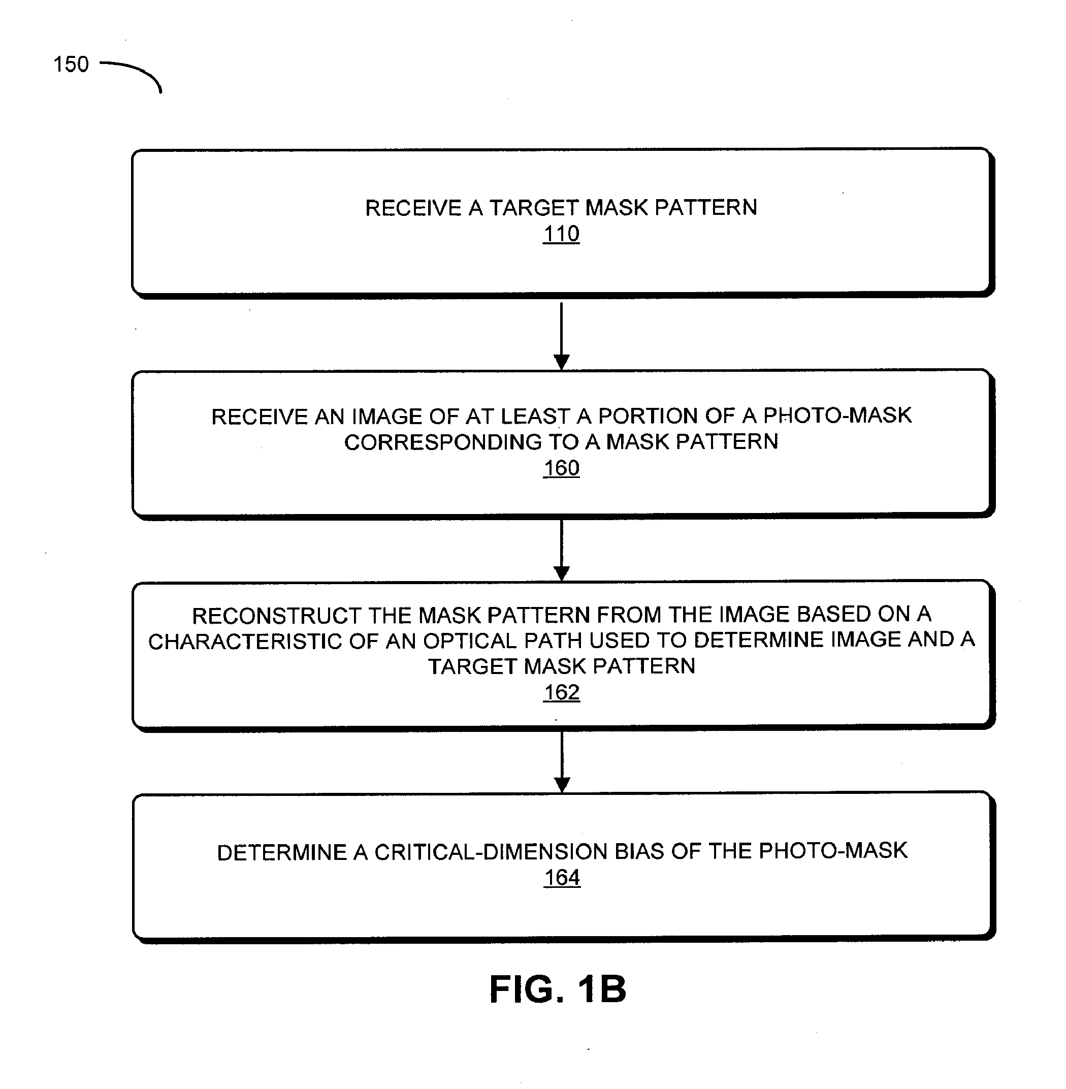
[0033]The following description is presented to enable any person skilled in the art to make and use the invention, and is provided in the context of a particular application and its requirements. Various modifications to the disclosed embodiments will be readily apparent to those skilled in the art, and the general principles defined herein may be applied to other embodiments and applications without departing from the spirit and scope of the present invention. Thus, the present invention is not intended to be limited to the embodiments shown, but is to be accorded the widest scope consistent with the principles and features disclosed herein.

[0034]Embodiments of a computer system, a method, and a computer program product (i.e., software) for use with the computer system are described. These devices and processes may be used to reconstruct a mask pattern corresponding to a photo-mask using a target mask pattern (which excludes defects) and an image of at least a portion of the photo...


PUM


Abstract

A technique for reconstructing a mask pattern corresponding to a photo-mask using a target mask pattern (which excludes defects) and an image of at least a portion of the photo-mask is described. This image may be an optical inspection image of the photo-mask that is determined using inspection optics which includes an optical path, and the reconstructed mask pattern may include additional spatial frequencies than the image. Furthermore, the reconstructed mask pattern may be reconstructed based on a characteristic of the optical path (such as an optical bandwidth of the optical path) using a constrained inverse optical calculation in which there are a finite number of discrete feature widths allowed in the reconstructed mask pattern, and where a given feature has a constant feature width. Consequently, the features in the reconstructed mask pattern may each have the constant feature width, such as an average critical dimension of the reconstructed mask pattern.

Description

BACKGROUND OF THE INVENTION[0001]1. Field of the Invention[0002]The present invention relates to techniques for inspecting and qualifying a photo-mask. More specifically, the invention relates to a technique for determining whether or not a photo-mask is acceptable by reconstructing a mask pattern of the photo-mask from a lower resolution image.[0003]2. Related Art[0004]Photolithography is a widely used technology for producing integrated circuits. In this technique, a light source illuminates a photo-mask. The resulting spatially varying light pattern is projected on to a photoresist layer on a semiconductor wafer by an optical system (referred to as an ‘exposure tool’). By developing the 3-dimensional pattern produced in this photoresist layer, a layer in the integrated circuit is created. Furthermore, because there are often multiple layers in a typical integrated circuit, these operations may be repeated using several photo-masks to produce a product wafer.[0005]Unfortunately, a...

Claims


Application Information

Patent Timeline
Patent Type & Authority Applications(United States)
IPC IPC(8): G06F17/50
CPCG03F1/68G03F1/36
Inventor PANG, LINYONG
Owner KLA TENCOR TECH CORP
Why Eureka
Try Eureka