Light emitting device

Active Publication Date: 2012-06-07
SUZHOU LEKIN SEMICON CO LTD
View PDF4 Cites 3 Cited by
  • Summary
  • Abstract
  • Description
  • Claims
  • Application Information

AI Technical Summary

Benefits of technology

[0006]An embodiment is to provide a light emitting device in which a buffer layer of a rock salt structured nitride is disposed between a light emitting structure and a sapphire substrat

Problems solved by technology

In the meantime, though the light emitting device may be fabricated to include a nitride semiconductor layer formed on

Method used


Image

  • Light emitting device
  • Light emitting device
  • Light emitting device

Examples


Embodiment Construction

[0028]Hereinafter, embodiments will be described with reference to the annexed drawings.

[0029]It will be understood that, when an element is referred to as being ‘on’ or “under” another element, it can be directly on / under the element, and one or more intervening elements may also be present. When an element is referred to as being ‘on’ or ‘under’, ‘under the element’ as well as ‘on the element’ can be included based on the element.

[0030]A thickness or size of an element shown in a drawing may be exaggerated, omitted or shown schematically for convenience or clarity of description. And, the size of the element may not be shown to scale, perfectly.

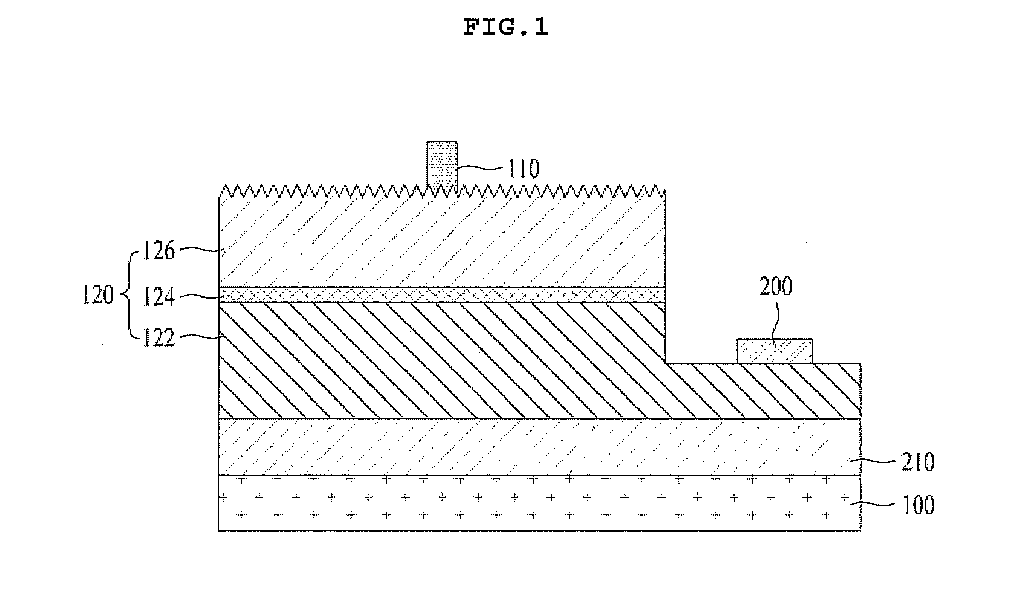
[0031]FIG. 1 illustrates a cross-sectional view of a light emitting device in accordance with an embodiment.

[0032]Referring to FIG. 1, the light emitting device may include a buffer layer 210, a light emitting structure 120, and first and second electrodes 200 and 110. The buffer layer 210 is disposed on a substrate 100, and the light emitt...


PUM


Abstract

Embodiments disclose a light emitting device including a substrate, a buffer layer disposed on an R-plane of the substrate, the buffer layer having a rock salt structured nitride, and a light emitting structure arranged on the buffer layer, the light emitting structure being grown in an a-plane.

Description

CROSS REFERENCE TO RELATED APPLICATION[0001]This application claims priority under 35 U.S.C. §119 to Korea Application No. 10-2011-0087852 filed in Korea on 31 Aug. 2011 which is hereby incorporated in its entirety by reference as if fully set forth herein.TECHNICAL FIELD[0002]Embodiments relate to a light emitting device.BACKGROUND[0003]The light emitting device, such as a light emitting diode of III-V group or II-VI group compound semiconductor or a laser diode, can produce various colors, such as red, blue, and ultra-violet owing to development of the thin film growth technology and device materials therefor, as well as a white color of good efficiency by using a fluorescent material or mixing colors, and is advantageous in that the light emitting device has power consumption lower than the present light sources, such as a fluorescent light and an incandescent light, a semi-permanent lifetime, fast response speed, and safety, and is environment friendly.[0004]Accordingly, applica...

Claims


Application Information

Patent Timeline
IPC IPC(8): H01L33/32H01L33/34
CPCH01L21/0237H01L21/0242H01L21/02433H01L21/02439H01L21/02488H01L21/02521H01L21/0254H01L2224/48091H01L33/12H01L33/16H01L33/32H01L2924/00014
Inventor SHIM, HEEJAE
Owner SUZHOU LEKIN SEMICON CO LTD
Why Eureka
Try Eureka