Preparation of AlN growth face composite substrate and nitride semiconductor device

A technology of nitride semiconductors and composite substrates, which is applied in semiconductor/solid-state device manufacturing, single crystal growth, crystal growth, etc., can solve the problems of high price, limit the wide application of devices, and high dislocation density, and reduce lattice loss. matching, good optical and electrical properties, and small lattice mismatch

Inactive Publication Date: 2009-08-12
XIAMEN UNIV
View PDF3 Cites 2 Cited by
  • Summary
  • Abstract
  • Description
  • Claims
  • Application Information

AI Technical Summary

Problems solved by technology

[0003] At present, the key factor restricting the development of Group III nitride materials and devices is the lack of lattice-matched and reasonably priced epitaxial substrates. For example, there is a relatively large lattice mismatch between commonly used sapphire substrates and Group III nitrides. As a result, the crystal quality of the nitride epitaxial layer is not high, and the dislocation density is as high as 10 10 / cm 2 , which limits the performance of nitride devices; the lattice mismatch between silicon carbide substrate materials and group III nitrides is small, but the price is extremely expensive, which limits the wide application of devices

Method used


Image

  • Preparation of AlN growth face composite substrate and nitride semiconductor device

Examples


Embodiment Construction

[0016] The following embodiments will further illustrate the present invention in conjunction with the accompanying drawings.

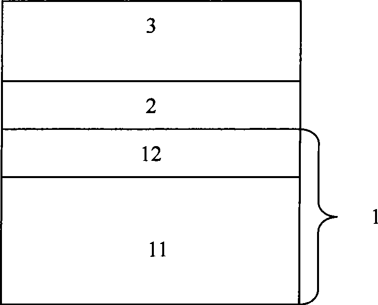
[0017] like figure 1 As shown, a metal-organic chemical vapor deposition system is used to grow a composite substrate 1 with an AlN growth surface, a transition layer 2 and a nitride semiconductor structural material layer 3, wherein the composite substrate 1 with an AlN growth surface includes a sapphire substrate 11 and An AlN epitaxial layer 12 is grown on the substrate. Trimethylgallium (TMGa), trimethylaluminum (TMA1) and trimethylindium (TMIn) were used as Group III sources during the growth process, and high-purity ammonia (NH 3 ) as the V group source, high-purity hydrogen and nitrogen as the carrier gas, magnesium dicene (CP 2 Mg) and high-purity silane (SiH 4 ) as the doping source. Place the sapphire substrate 11 in the growth system, heat it to 1000-1200° C. with hydrogen gas, and keep the high temperature for 10 minutes to remove the ...


PUM

PropertyMeasurementUnit
thicknessaaaaaaaaaa
thicknessaaaaaaaaaa

Abstract

The invention discloses a preparation method for an AlN growth face composite substrate and a nitride semiconductor device, relates to a nitride semiconductor material, and provides a preparation method f an AlN growth face composite substrate for growing the nitride semiconductor material and a nitride semiconductor device. An AlN epitaxial layer grows on a substrate to obtain the AlN growth face composite substrate. The nitride semiconductor device is provided with the AlN growth face composite substrate, a transition layer and a nitride semiconductor device structural material layer. The transition layer grows on the AlN growth face composite substrate and consists of a nitride material AlxInyGa(1-x-y)N(x is more than 0 and less than or equal to 1, and y is more than or equal to 0 and less than or equal to 1.) containing Al. The nitride semiconductor device structural material layer grows on the transition layer, comprises an n-shaped layer, luminescent and absorbing functional structural layers and a p-shaped layer, and contains the component of the AlxInyGa(1-x-y)N(x is more than 0 or equal to and less than or equal to 1, and y is more than or equal to 0 and less than or equal to 1.).

Description

technical field [0001] The invention relates to a nitride semiconductor material, in particular to a preparation method of an AlN growth plane composite substrate and a nitride semiconductor device prepared on the AlN growth plane composite substrate. Background technique [0002] Group III nitride semiconductor materials are the third generation developed rapidly after the first-generation element semiconductors silicon (Si) and germanium (Ge), the second-generation compound semiconductors gallium arsenide (GaAs), indium phosphide (InP), etc. A typical representative of semiconductor materials. Compared with other material systems, GaN has the advantages of wide direct bandgap, high critical breakdown voltage, high saturation drift velocity, high thermal conductivity, and high chemical and thermal stability. Group III nitride semiconductors include GaN, InN, AlN and their alloys. The band gap is continuously adjustable in the range of 0.7-6.28eV. It is an excellent materia...

Claims


Application Information

Patent Timeline
Patent Type & Authority Applications(China)
IPC IPC(8): C30B29/40C30B29/38C30B25/02H01L21/205H01L21/08
Inventor 康俊勇李书平陈航洋刘达艺杨伟煌林伟李金钗
Owner XIAMEN UNIV
Why Eureka
Try Eureka