Silicon-based micro LED chip and manufacturing method thereof

A technology of LED chips and manufacturing methods, which is applied in the direction of electrical components, electric solid devices, circuits, etc., can solve the problems of damage to GaN materials and Micro LED chips, affect the reliability of LED chips, and chip leakage, so as to reduce lattice mismatch, Conducive to matching adjustment and improving the effect of crystal quality

Pending Publication Date: 2020-02-28
FOSHAN NATIONSTAR SEMICON
View PDF0 Cites 2 Cited by
  • Summary
  • Abstract
  • Description
  • Claims
  • Application Information

AI Technical Summary

Problems solved by technology

However, this method of substrate removal is difficult to remove because GaN absorbs laser light and decomposes the N 2 Cause damage to GaN materials and MicroLED chips, resulting in chip leakage or breakage, greatly affecting the reliability of LED chips
In addition, after removing the sapphire substrate, Micro LED has far exceeded the precision limit of traditional cutting and splitting equipment due to its size less than 100 μm. Therefore, cutting and separation technology is also a major bottleneck restricting the development of Micro LED.

Method used


Image

  • Silicon-based micro LED chip and manufacturing method thereof
  • Silicon-based micro LED chip and manufacturing method thereof
  • Silicon-based micro LED chip and manufacturing method thereof

Examples


Embodiment Construction

[0044] In order to make the object, technical solution and advantages of the present invention clearer, the present invention will be further described in detail below in conjunction with the accompanying drawings.

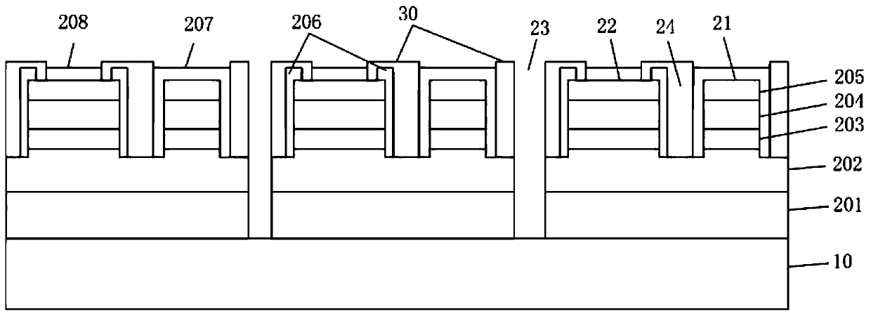
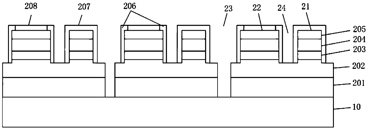
[0045] see figure 1 , a silicon-based micro-LED chip provided by the present invention includes a silicon substrate 10, several light-emitting structures 20, cutting grooves 23, and an organic insulating layer 30. The cutting grooves 23 are arranged between the light-emitting structures 20, and the light-emitting structures 20 apart.

[0046]The light emitting structure 20 includes an etch barrier layer 201, a first semiconductor layer 202, an active layer 203, a second semiconductor layer 204 and an isolation groove 24, and the etch barrier layer 201 is disposed on the silicon substrate 10 and the first semiconductor layer Between the layers 202 , the isolation groove 24 is etched to the first semiconductor layer 202 to divide the light emitting structure 20 int...


PUM

PropertyMeasurementUnit
thicknessaaaaaaaaaa

Abstract

The invention discloses a silicon-based micro LED chip and a manufacturing method thereof. The chip comprises a silicon substrate, a plurality of light emitting structures, cutting grooves and an organic insulating layer, wherein the cutting grooves are formed among the light emitting structures. The chip is advantaged in that the silicon substrate is adopted to replace a sapphire substrate, so damage to a gallium nitride material and a micro LED chip caused by N2 generated by decomposition after gallium nitride absorbs laser during laser stripping of the sapphire substrate is avoided, the silicon substrate is removed through a physical grinding and chemical corrosion two-step method, the light emitting structure can be protected against damage while the silicon substrate is effectively removed, and the removal yield and reliability of the substrate are improved.

Description

technical field [0001] The invention relates to the technical field of light emitting diodes, in particular to a silicon-based micro-LED chip and a manufacturing method thereof. Background technique [0002] At present, the mainstream screen display technologies are mainly concentrated on LCD and AMOLED. Among them, LCD has a long life, but needs backlight, and the contrast is not high, and it cannot be bent; The problem is mainly the problem of screen burn-in. [0003] For Micro LED, the chip size is less than 100 μm, and the size of a single chip is not even 1% of the original LED chip. The LED display is a high-density micro-scale micro-LED array integrated on a chip, and each pixel of the LED display can be addressed and individually driven to light up. The LED display is made of inorganic materials, and its lifespan and stability are significantly better than that of the AMOLED LED display, and it is not prone to screen burn-in and aging. At the same time, it also has...

Claims


Application Information

Patent Timeline
Patent Type & Authority Applications(China)
IPC IPC(8): H01L27/15H01L33/00
CPCH01L27/156H01L33/007
Inventor 徐亮雷自合
Owner FOSHAN NATIONSTAR SEMICON
Why Eureka
Try Eureka