InAs/AlSb high electron mobility transistor (HEMT) epitaxial structure and fabrication method thereof
An epitaxial structure, alasxsb1-x technology, applied in the field of microelectronics, can solve the problems of oxidation device performance, lattice mismatch high activity AlSb, drop, etc., to prevent AlSb layer oxidation, improve stability and reliability, and reduce costs Effect
- Summary
- Abstract
- Description
- Claims
- Application Information
AI Technical Summary
Problems solved by technology
Method used
Image
Examples
preparation example Construction
[0044] The embodiment of the present invention also provides a method for preparing an InAs / AlSb HEMT epitaxial structure, which specifically includes the following steps:
[0045] 1) A buffer layer 2 is grown on the substrate 1 by a plasma-enhanced chemical vapor deposition method, and the buffer layer 2 is a Si film with a thickness of 30-100 nm;
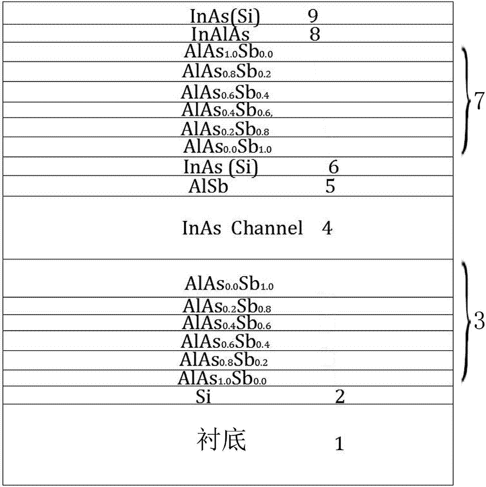
[0046] 2) Using MBE equipment, deoxidize the substrate with buffer layer 2 at 710°C and degas at 650°C for 3 minutes. When the temperature reaches 560°C, turn on the sources of Al, As and Sb, and adopt a stepwise variable composition growth method at Growth of AlAs on Si x Sb 1-x The lower barrier layer 3, in which the composition ratio of Al, As, and Sb is 1:X:1-X, and the value of X takes 6 values that decrease successively from 1 to 0, grows 6 layers from bottom to top, and each Layer thickness is 30-200nm;
[0047] 3) Using MBE equipment, in AlAs x Sb 1-x InAs channel layer 4 is grown on the lower barrier layer 3: when ...
Embodiment 1
[0057] The equipment used in the embodiment of the present invention includes: microelectronic process equipment such as molecular beam epitaxy MBE and plasma enhanced chemical vapor deposition PECVD.
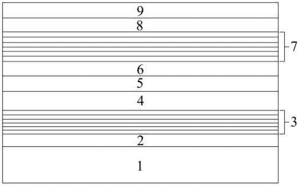
[0058] refer to figure 2 , an InAs / AlSb HEMT epitaxial structure provided by an embodiment of the present invention is formed according to the following structure, which specifically includes from bottom to top: a substrate 1, a buffer layer 2, an AlAsxSb1-x lower barrier layer 3, and an InAs trench Channel layer 4, AlSb spacer layer 5, InAs doped layer 6, AlAs x Sb 1-x An upper potential barrier layer 7, an InAlAs hole blocking layer 8 and an InAs cap layer 9.
[0059] Specifically, in this embodiment, as figure 2 As shown, the outer surface of the flexible material is wrapped with a thickness of 100nm SiO 2 , forming the substrate 1, the so-called flexible substrate; the SiO used for the substrate 1 wrapping 2 A thickness of 30nmSi is grown on it to form a buffer layer...
PUM
 Abstract
Description
Claims
Application Information

