

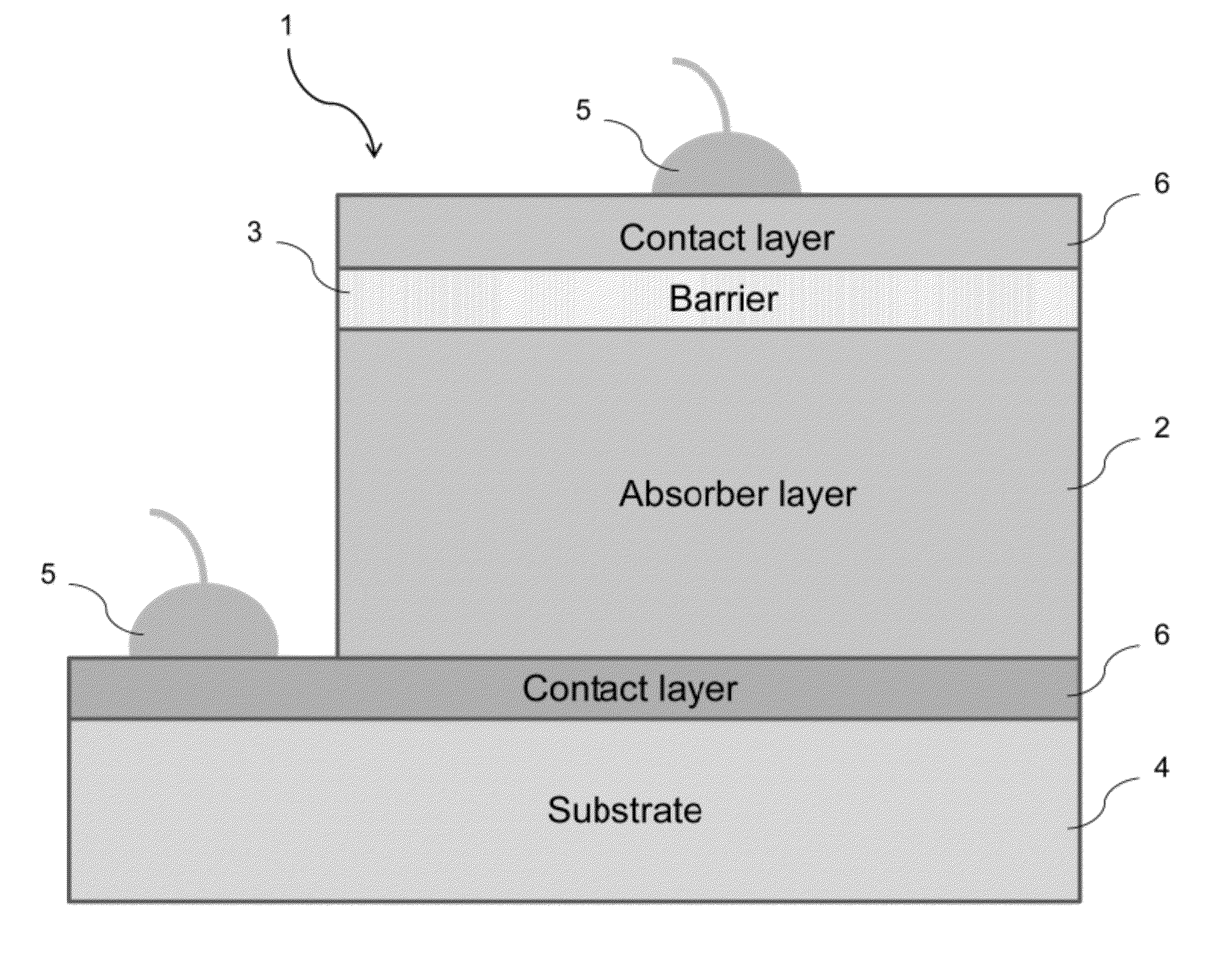
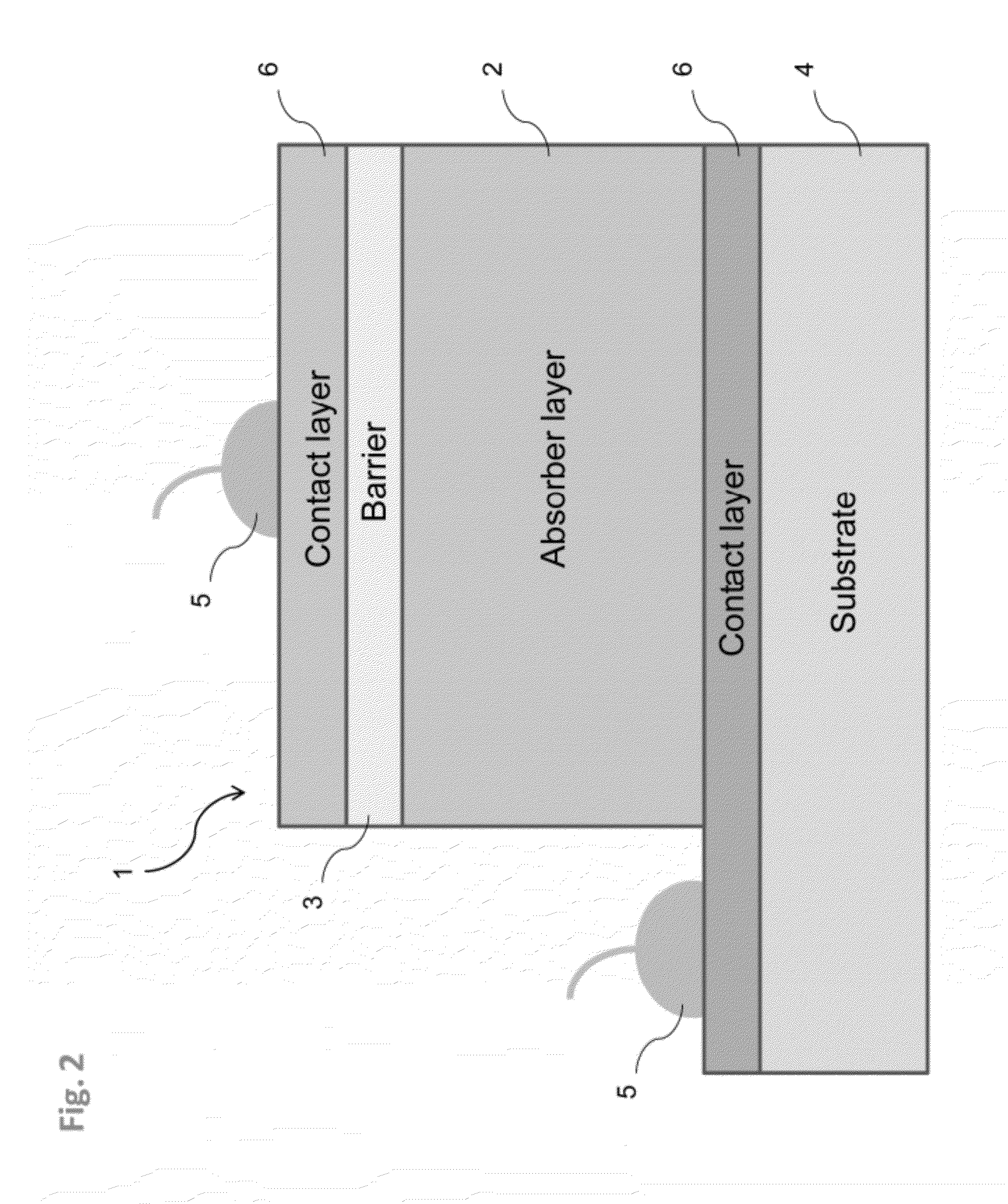
Barrier infrared detector
a technology of infrared detector and carrier, which is applied in the field of infrared detector, can solve the problems of not reaching very high performance levels, still having limited spectral range, and building a high-performance infrared photodetector that requires considerable sophistication, and achieves the effect of minimal strain
- Summary
- Abstract
- Description
- Claims
- Application Information
AI Technical Summary
Benefits of technology
Problems solved by technology
Method used
Image

Examples
example 1
nBn Detector Performance Testing
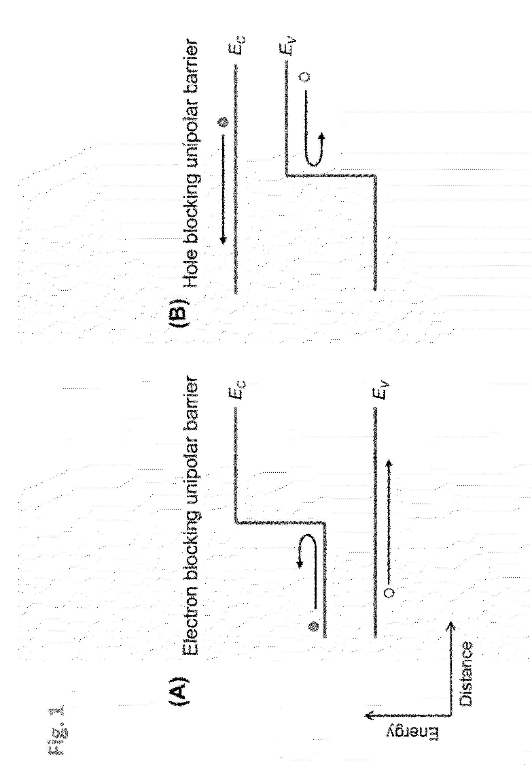
[0138]FIG. 14 shows the schematic energy band diagram of on exemplary embodiment of a high-performance barrier infrared detector in accordance with the current invention, using a strain-balanced n-type InAs / InSbAs superlattice as the infrared absorber and the top contact layer, and a matching AlAsSb electron blocking unipolar barrier. The detector shows excellent material quality (FIG. 15), covering the key infra-red atmospheric transmission window of between 3 and 5 microns having cutoff wavelengths of greater than 5.3 microns (FIG. 16), and has excellent dark current characteristics operating at 150 K.
[0139]In particular, FIG. 15 provides a rank plot (of 18 devices) made in accordance with the current invention. As shown, the plot shows the devices have a R0A (zero bias differential resistance-area product) ˜10,000 ohm-cm2 at a temperature of T=150K, and that most of the large-area 200 μm×200 μm devices are free of defects. The lack of defects provi...
example 2
Dual-Band nBn Detector
[0141]FIG. 19 shows the schematic energy band diagram of an exemplary embodiment of a dual-band nBn detector structure, consisting of an electron-blocking graded-gap unipolar barrier sandwiched between two absorber superlattices with different energy band gaps (hence different cutoff wavelengths) in accordance with the current invention. In such an embodiment, the two absorber superlattices could be made from strain-balanced n-type InAs / InAsSb superlattices with the same InAsSb alloy composition, but different periodicities. Similarly, the electron-blocking graded-gap unipolar barrier could be made from a 4-layer AlSb / AlAa / AlSb / GaSb superlattice with varying GaSb layer width as described earlier to smoothly bridge the valence band edges of the two absorbers superlattices.
example 3
Dual-Band pBp Detector
[0142]FIG. 20 shows the schematic energy band diagram of an exemplary dual-band pBp detector structure, consisting of a hole-blocking graded-gap unipolar barrier sandwiched between two p-type absorber superlattices with different energy band gaps in accordance with the current invention. In such an embodiment, the barrier and the two absorbers could all be made from InAs / InAsSb superlattices with the same InAsSb alloy composition, but different periodicities. Alternatively, the barrier could be made from an InAs / AlSb superlattice or an InAsSb / AlAsSb superlattice.
PUM
 Abstract
Description
Claims
Application Information