

Semiconductor device having different fin widths
a technology of mikro-conductor and fin, applied in the direction of mikro-conductor devices, transistors, electrical apparatus, etc., can solve the problems of gate resistance limitation gain, increase noise in rf circuits, increase the harmonic distortion of signals in amplifier circuits,
- Summary
- Abstract
- Description
- Claims
- Application Information
AI Technical Summary
Benefits of technology
Problems solved by technology
Method used
Image

Examples
Embodiment Construction
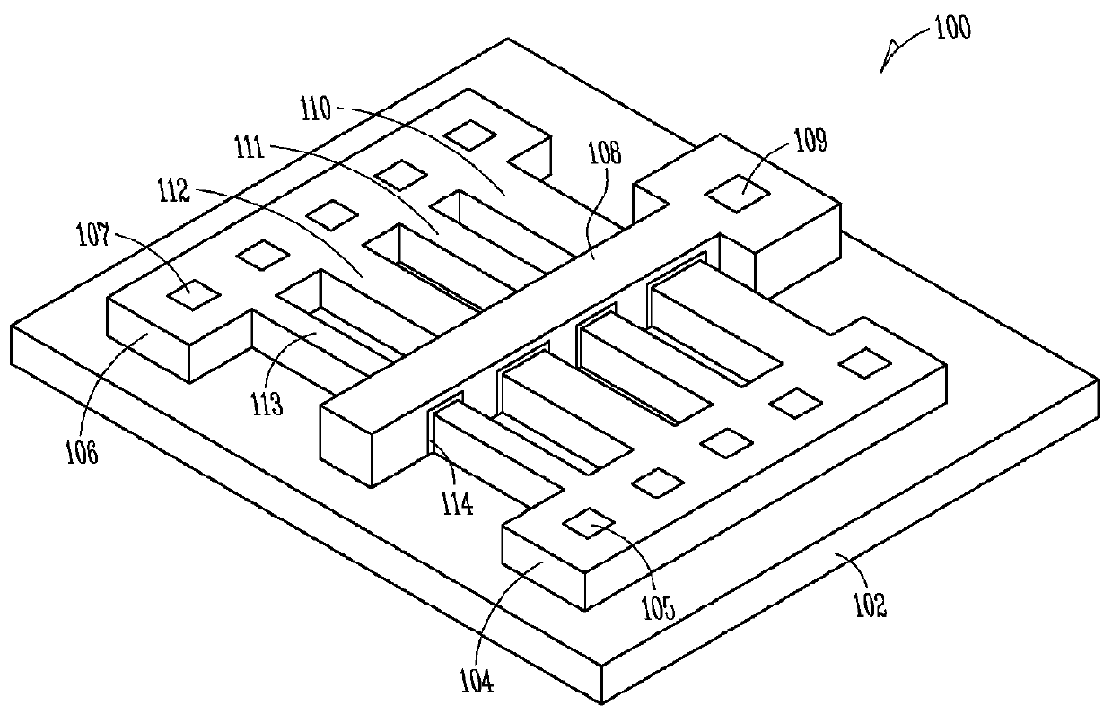
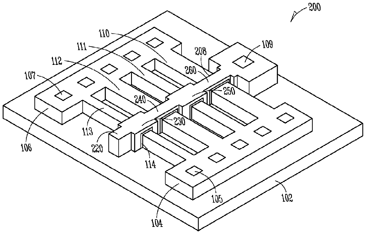
[0034]The following detailed description refers to the accompanying drawings that show, by way of illustration, specific details and embodiments in which the invention may be practiced. These embodiments are described in sufficient detail to enable those skilled in the art to practice the invention. Other embodiments may be utilized and structural, logical, and electrical changes may be made without departing from the scope of the invention. The various embodiments are not necessarily mutually exclusive, as some embodiments can be combined with one or more other embodiments to form new embodiments. In this document, the terms “a” or “an” are used, as is common in patent documents, to include one or more than one. In this document, the term “or” is used to refer to nonexclusive or, such that “A or B” includes “A but not B,”“B but not A,” and “A and B,” unless otherwise indicated.
[0035]The term “substrate” is understood to include a semiconductor wafer. The term “substrate” is also us...
PUM
 Abstract
Description
Claims
Application Information