Radiofrequency amplifier

a radiofrequency amplifier and amplifier technology, applied in amplifiers with semiconductor devices/discharge tubes, amplifier modifications to extend bandwidth, semiconductor devices, etc., can solve the problems of large distortions due to memory effects, particularly problematic memory effects, etc., to improve bandwidth, reduce memory effects, and facilitate load line modulation conditions

Active Publication Date: 2012-06-14
AMPLEON NETHERLANDS
View PDF4 Cites 27 Cited by
  • Summary
  • Abstract
  • Description
  • Claims
  • Application Information

AI Technical Summary

Benefits of technology

[0006]An aspect of the invention is that high inductances are not required inside the device package or on the active device, and therefore losses within the package can be reduced and the overall size of the package minimised.
[0007]The amplifier according to the invention has no need for a high value shunt inductance inside the device package, and therefore the number of bond wires connecting the drain of the active device with the second output lead can be greatly increased, which greatly extends the applicability of the invention for high power amplifiers.
[0010]The use of a post-matching network comprising a high pass network partly provided on the amplifier die with a low pass network provided off the amplifier die allows for a wideband impedance transformation at zero phase shift at central frequency. This avoids any detrimental impedance inversion between the channel (the drain or collector) of the active device and the discrete power device output, and also makes provision of load line modulation conditions easier when operating as a main or peak device in a Doherty amplifier.
[0011]The use of such a post-matching network also allows for an improved amplifier having a reduced memory effect and an improved bandwidth. Other aspects may include an improved broad band VBW, low phase rotation, a more compact form and lower loss.

Problems solved by technology

Memory effects are particularly problematic at frequencies of 1 GHz and above.
These memory effects result from parasitic inductances between the power supply and the amplifier and from the speed of variation and magnitude of current consumption by the amplifier, which follows the envelope of the input signal modulation.
At higher modulation frequencies larger distortions tend to appear due to such memory effects.

Method used


Image

  • Radiofrequency amplifier
  • Radiofrequency amplifier
  • Radiofrequency amplifier

Examples


first embodiment

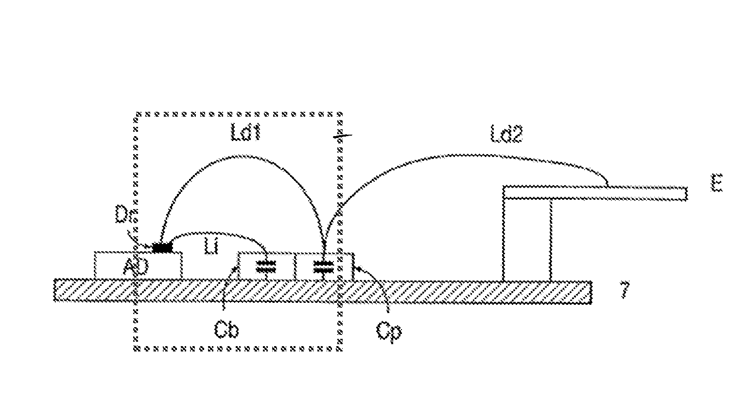
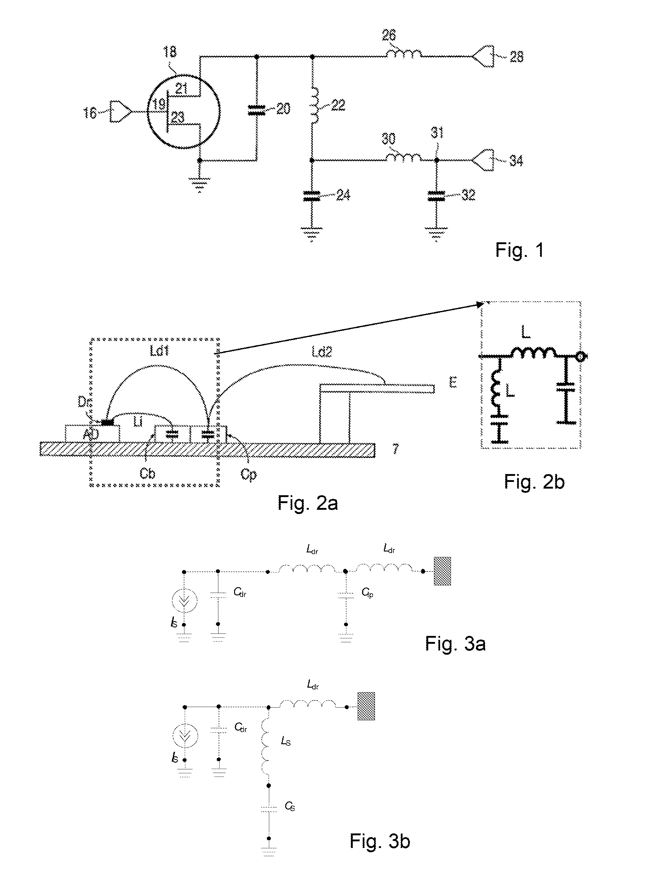
[0040]A first exemplary embodiment of a radiofrequency amplifier 500 in accordance with the invention is illustrated in FIGS. 5a, 5b and 5c. FIG. 5a illustrates a schematic sectional view of the amplifier, FIG. 5b a schematic circuit diagram of the amplifier 500 and FIG. 5c a perspective view of the physical arrangement of the amplifier 500. Each of these diagrams show an active device AD 501 having an output 502 connected to a first RF output lead 503 via a first bond wire Ld BW 504, and to a second output lead 505 via a second bond wire Ls BW 506, each bond wire providing an inductance between the amplifier output 502 and the output leads 503, 505. In this illustrated embodiment the output 502 of the active device 501 is the drain connection of the active device 501.

[0041]This implementation is similar to known post matching circuits for RF power amplifiers in which a built-in shunt inductance (or ‘inshin’) is used to cancel the output capacitance Cds 507 of the amplifier element ...

second embodiment

[0046]A second embodiment of a radiofrequency amplifier 600 in accordance with the invention is illustrated in FIGS. 6a, 6b and 6c. FIG. 6a illustrates a schematic sectional view of the amplifier 600, FIG. 6b a schematic circuit diagram and FIG. 6c a general perspective view of the physical arrangement of the amplifier 600.

[0047]The main difference with respect to the first embodiment described above and illustrated in FIGS. 5a-5c is the addition of a series capacitor Cser 621 to the output of the active device 501 (601 in FIGS. 6a and 6c). All other components of the amplifier 600 are otherwise as described above in relation to the first embodiment. The series capacitor 621 can be provided either on the active device 601 as part of the output as shown in FIGS. 6a and 6c or, as shown in FIG. 6b, on a separate die. The series capacitor 621 acts to compensate for the inductance of the first output RF lead 503. This is particularly advantageous for so-called “gull wing” packages, where...

third embodiment

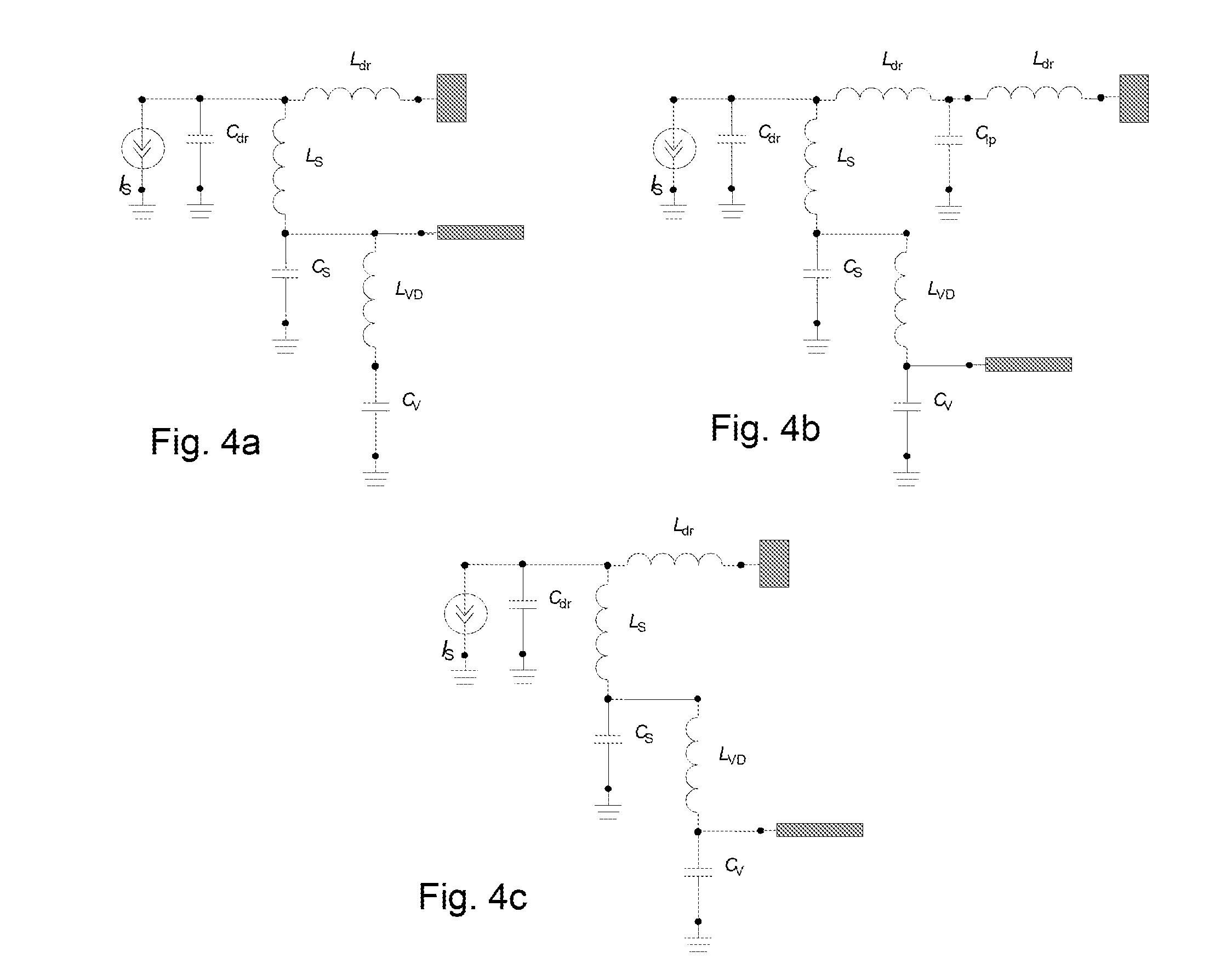
[0050]The amplifiers of either the first or second embodiments can be further improved through the use of a special transmission line instead of through the simple metal strip forming the second output lead of the first and second embodiments.

[0051]At frequencies close to 1 Ghz the inductance introduced by extra leads and the PCB can reach values which are not usable for post match and video decoupling, due to the value of the parasitic inductance between the ground connections of the PCB and the active die (as described above in relation to FIG. 5b). In order to minimize this parasitic inductance, a special transmission line may be used instead of the simple metal strip inside the amplifier package. Exemplary embodiments of such transmission lines are illustrated in FIGS. 8 and 9. FIG. 8 shows a series of plan views of three variations of a transmission line 801a, 801b, 801c based on a modified version of the second output lead of the first and second embodiments. The modified seco...


PUM


Abstract

The invention relates to high power radiofrequency amplifiers, in particular to amplifiers having output impedance matching networks, exemplary embodiments of which include a radiofrequency amplifier having an active device mounted on a substrate within a device package, the amplifier having an output impedance matching network comprising a high pass network provided at least partly on the active device and a low pass network having a first inductive shunt connection between an output of the active device and a first output lead and a second inductive shunt connection between the output of the active device and a second output lead, wherein part of the second output lead forms an inductance contributing to the inductance of the low pass network.

Description

[0001]This application claims the priority under 35 U.S.C. §119 of European patent application no. 10252098.8, filed on Dec. 10, 2010, the contents of which are incorporated by reference herein.FIELD OF THE INVENTION[0002]The invention relates to high power radiofrequency amplifiers, in particular to such amplifiers comprising output impedance matching networks.BACKGROUND OF THE INVENTION[0003]High power radiofrequency amplifiers, such as Doherty amplifiers as well as single-ended class AB amplifiers, tend to exhibit memory effects. Memory effects are particularly problematic at frequencies of 1 GHz and above. These memory effects result from parasitic inductances between the power supply and the amplifier and from the speed of variation and magnitude of current consumption by the amplifier, which follows the envelope of the input signal modulation. Such parasitic inductances may exist as part of a power supply network. At higher modulation frequencies larger distortions tend to app...

Claims


Application Information

Patent Timeline
Patent Type & Authority Applications(United States)
IPC IPC(8): H03F1/00
CPCH01L23/66H01L2924/30107H01L2223/6655H03F1/42H01L2224/48091H01L2223/6611H01L2924/19107H01L2224/48247H01L2924/3011H01L2924/3025H01L2224/48137H01L2224/49109H01L2924/00014H01L2924/00H01L2924/30111H03F1/565H03F3/195
Inventor BLEDNOV, IGORVOLOKHINE, IOURI
Owner AMPLEON NETHERLANDS
Why Eureka
Try Eureka