Wiring board and method of manufacturing the same

Inactive Publication Date: 2012-06-21
NGK SPARK PLUG CO LTD
View PDF10 Cites 10 Cited by
  • Summary
  • Abstract
  • Description
  • Claims
  • Application Information

AI Technical Summary

Benefits of technology

[0024]Embodiments of the wiring board of the present invention allow for the high-density packaging of conductor posts 16. That is, the wiring boards 10 may have conductor posts 16 with larger aspect ratios (proportion of height to width) than those in the related art. Accordingly, even for conductor posts 16 with small pitches, sufficient height from the surface of the solder resist layer can be attained. Furthermore, high connection reliability can be achieved between the wiring board 10 and a part to be packaged in this wiring board 10 by using a conductor post 16.
[0034]In the case where the conductor post 16 composed of tin and is plated within both the first through-hole 131 and a second through-hole 151 in a conductor post forming process PR7, and a conductor post heating process PR10 of heating the conductor post 16 is included after a photoresist layer removing process PR8, the wiring board 10 has highly accurate conductor post 16 positional and excellent joining strength between the conductor post 161 and the conductor layer 12a.

Problems solved by technology

The formation of bumps having high aspect ratios required for the foregoing high-density packaging is relatively difficulty.
However, in the case where a solder resist layer 13 is thick or in the diameter of a through-hole 131 formed in the solder resist layer 13 is small, the fabrication of the mask 22 per se is difficult, and it is also difficult to sufficiently ensure its precision.

Method used


Image

  • Wiring board and method of manufacturing the same
  • Wiring board and method of manufacturing the same
  • Wiring board and method of manufacturing the same

Examples


embodiment

[0122]The wiring board 10 of the invention is more specifically described below with respect to the following specific Embodiment, but it should not be construed that the invention is limited to this Embodiment.

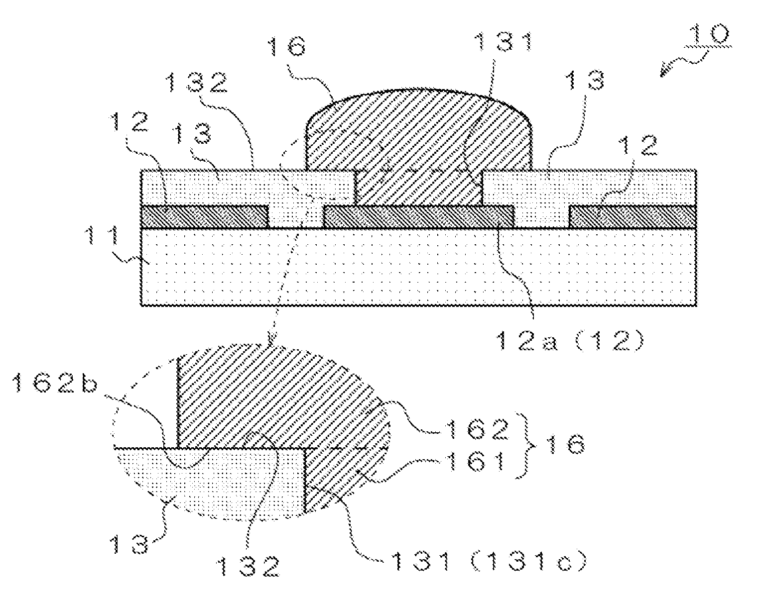
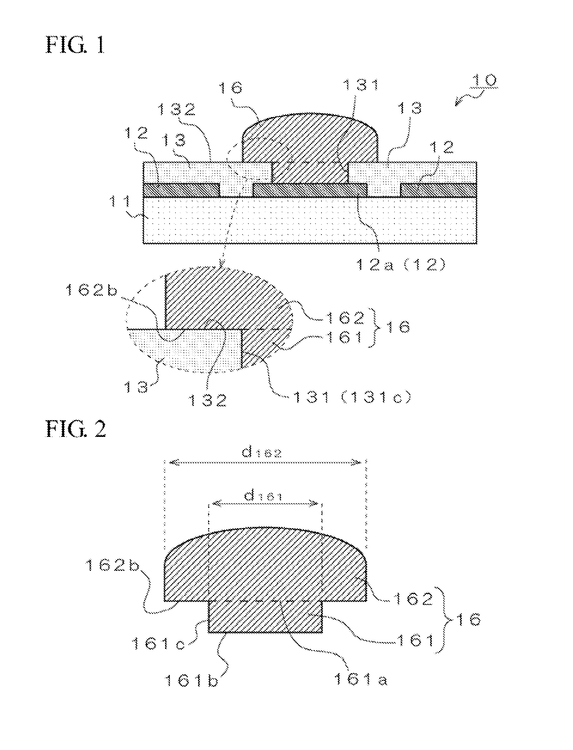
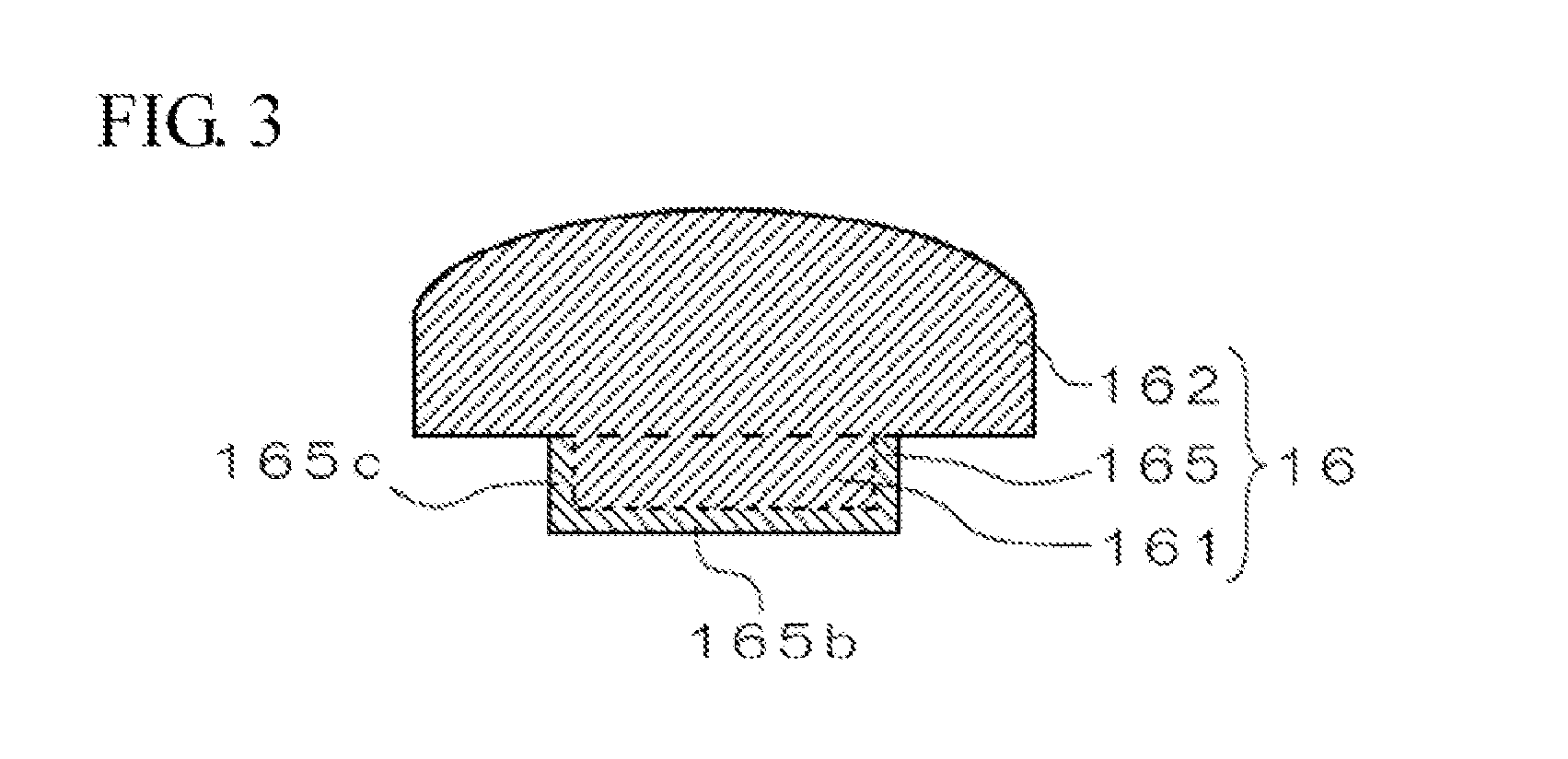
[0123](1) Wiring Board 10:

[0124]A wiring substrate 10 (see FIG. 1) which is manufactured according to this Embodiment includes a conductor layer 12 laminated on the side of one surface of a core substrate 11, a solder resist layer 13 laminated on this conductor layer 12, and a conductor post 16 that is electrically connected to a conductor layer 12a which is disposed in a lower portion of a through-hole 131 provided in the solder resist layer 13.

[0125]The core substrate 11 comprises glass epoxy (epoxy resin containing glass fibers as a core material) having a thickness of 0.8 mm. Also, the conductor layer 12 is obtained by patterning a copper foil having a thickness of 12 μm on one surface of the core substrate 11.

[0126]Furthermore, the solder resist layer 13 has a thickness ...


PUM

PropertyMeasurementUnit
Electrical conductivityaaaaaaaaaa

Abstract

A wiring board including a conductor post corresponding to high-density packaging is provided. The wiring board may comprise a conductor layer, a solder resist layer laminated on the conductor layer, and a conductor post that is electrically connected to a conductor layer which is disposed in a lower portion of a through-hole provided in the solder resist layer, wherein the solder resist layer comprises a thermosetting resin; the conductor post comprises tin, copper, or a solder; the conductor post includes a lower conductor post, which is located within the through-hole and includes an external side surface and a lower end surface, and an upper conductor post, which is located above the lower conductor post and is projected outside the solder resist layer; and at least a part of a lower end surface of the upper conductor post is brought into intimate contact with an outer surface of the solder resist layer.

Description

CROSS-REFERENCE TO RELATED APPLICATIONS[0001]The present application claims priority from Japanese Patent Application No. 2010-279706, which was filed on Dec. 15, 2010, the disclosure of which is herein incorporated by reference in its entirety.BACKGROUND OF THE INVENTION[0002]1. Field of the Invention[0003]The present invention relates to wiring boards and methods of manufacturing the same. In more detail, embodiments of the present invention relate to wiring boards having a conductor post and methods of manufacturing such wiring boards.[0004]2. Description of Related Art[0005]In recent years, as a high-density packaging technique, for example, a C4 (controlled collapse chip connection) method has been adopted. Wiring boards utilized in C4 methods have surface that is covered by a solder resist layer, and wherein a bump (conductor post) is vertically arranged, in an optionally bored opening in the solder resist layer, and electrically connected to a conductor layer within the wirin...

Claims


Application Information

Patent Timeline
IPC IPC(8): H05K1/09B23K31/02H05K3/00
CPCB23K1/0016B23K2201/42H01L21/4853H01L23/49816H01L24/16H05K2203/054H05K3/244H05K3/3473H05K3/4007H05K2201/0341H05K2201/0367H01L2224/16225B23K2101/42H05K3/34H01L23/12
Inventor YAMADA, ERINAHIGO, KAZUNAGASATO, HIRONORI
Owner NGK SPARK PLUG CO LTD
Why Eureka
Try Eureka