

Semiconductor device with decoupling capacitors mounted on conductors
- Summary
- Abstract
- Description
- Claims
- Application Information
AI Technical Summary
Benefits of technology
Problems solved by technology
Method used
Image

Examples
first embodiment
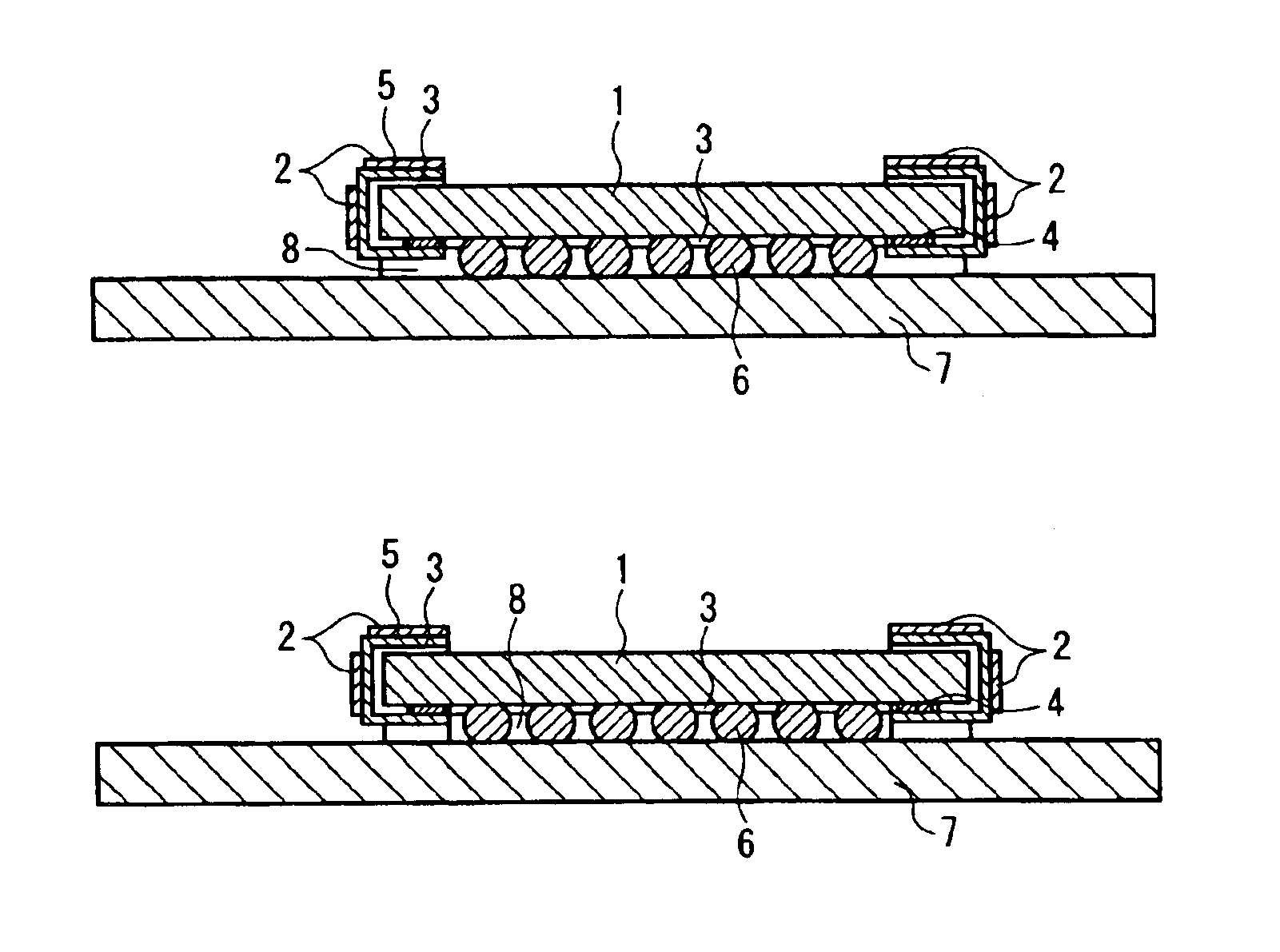
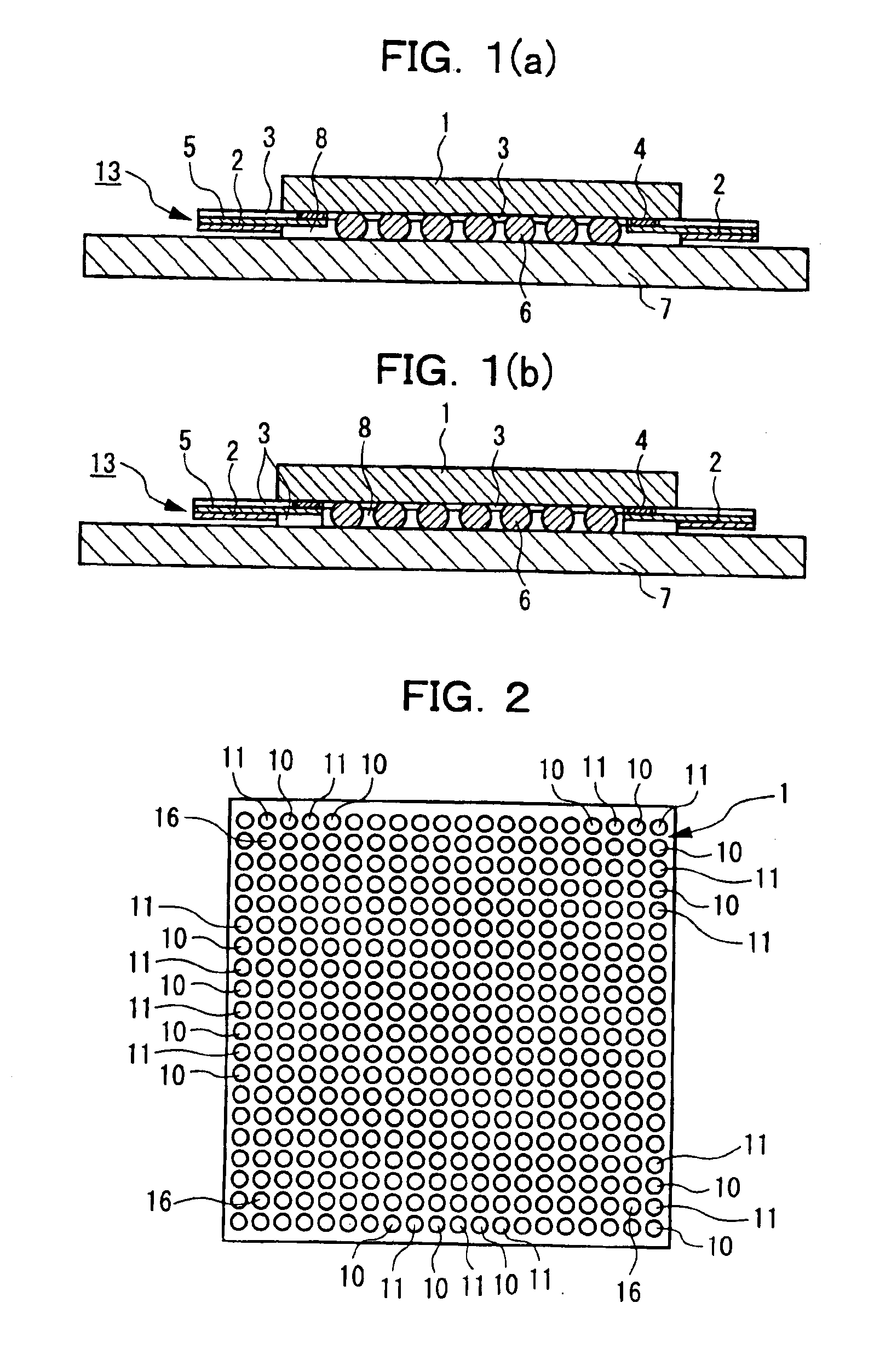
[0061]Specifically, the present invention is described below, with references made to FIG. 1 through FIG. 7.
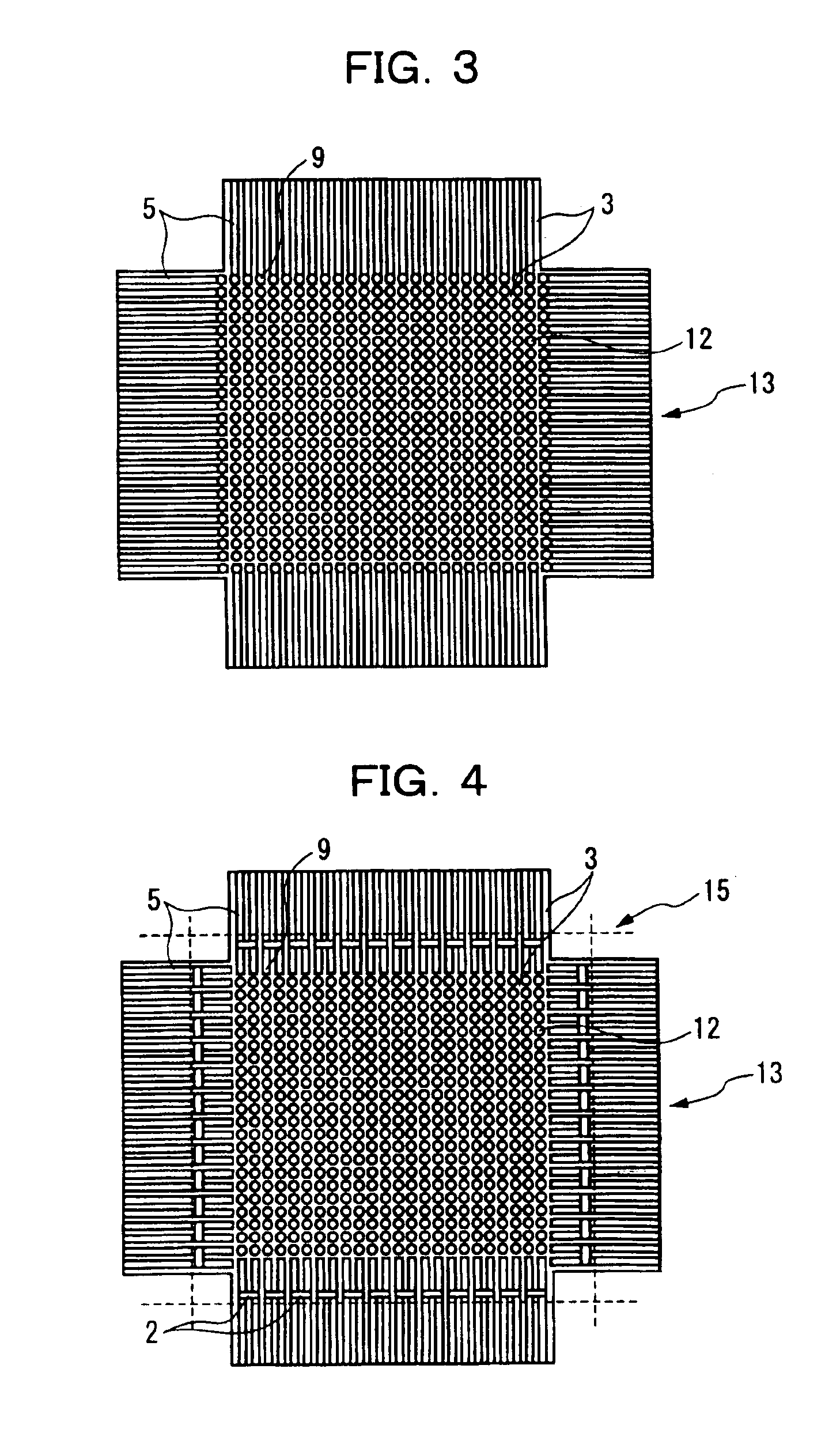
[0062]In the semiconductor device of this first embodiment, a flexible substrate is joined to the surface (circuit-formation surface) of an LSI device, FIG. 1(a) and FIG. 1(b) being cross-sectional views showing the condition of mounting a semiconductor device of this embodiment to a circuit board, FIG. 2 is a plan view showing the circuit-formation surface of an LSI device, FIG. 3 is a plan view showing the plane of connection between a flexible substrate and an LSI device, FIG. 4 is a plan view showing the condition of the decoupling capacitors mounted to the flexible substrate of FIG. 3, FIG. 5 is a plan view showing the circuit-formation surface of another example of an LSI device (main LSI device), this being referred to as the front surface thereof, and the opposite surface of the LSI device being referred to as the rear surface thereof hereinafter, FIG. 6 is a plan view...
third embodiment
[0079]the present invention is described below, with references made to FIG. 11 and FIG. 12.
[0080]FIG. 11(a) and FIG. 11(b) are cross-sectional views showing the condition of a semiconductor device according to this embodiment mounted to a circuit board, FIG. 12(a) and FIG. 12(b) are side views of the LSI device according to this embodiment. FIG. 12(a) shows an LSI device corresponding to the LSI device of the first embodiment shown in FIG. 1, while FIG. 12(b) shows an LSI device corresponding to the LSI device of the first embodiment shown in FIG. 5. The LSI device of this embodiment also uses a flexible substrate, and the basic configuration is the same as that of the first embodiment, the difference in this case being that the metal foil leads are bent to the side surface of the LSI device. Given this similarity, elements of FIG. 11 and FIG. 12 similar to elements of FIG. 1 through FIG. 7 are assigned the same reference numerals, and are not explicitly described herein.
[0081]In t...
fifth embodiment
[0086]the present invention is described below, with references made to FIG. 14 through FIG. 18.
[0087]In place of the flexible substrate used in the embodiments described above, a LSI device according to the fifth embodiment of the present invention makes use of a lead frame joined to the rear surface (circuit-formation surface) of the LSI device (main semiconductor device). FIG. 14(a) and FIG. 14(b) are cross-sectional views showing the condition of this semiconductor device mounted to a circuit board, and FIG. 15 is a plan view showing the plane of connection between the lead frame and the LSI device. Because the basic configuration is similar to that of the first embodiment, in the drawings referenced below, elements in common with elements in FIG. 1 through FIG. 7 are assigned the same reference numerals.
[0088]As shown in FIG. 14(a) and FIG. 14(b), the semiconductor device according to the fifth embodiment is basically formed by the LSI device 1, the lead frame 14, and the decou...
PUM
 Abstract
Description
Claims
Application Information