Circuitized substrate with dielectric interposer assembly and method

a dielectric interposer and circuitized substrate technology, applied in the direction of resistor details, resistor coating, printed resistor incorporation, etc., can solve the problem of restrictive connection of resistive paste between respective pairs of conductors

Inactive Publication Date: 2012-06-21
TTM TECH NORTH AMERICA LLC
View PDF24 Cites 23 Cited by
  • Summary
  • Abstract
  • Description
  • Claims
  • Application Information

AI Technical Summary

Benefits of technology

[0039]The present invention is directed to a circuitized substrate and a dielectric interposer, and more particularly, a drilled dielectric interposer and the placement of a resistor material between two or more subassembly circuitized substrate conductive points to allow individual resistive values to be employed for individual conductive junctions created between the subassemblies upon lamination.

Problems solved by technology

A void is formed by drilled holes and results in resistive paste connections being restrictively formed between respective pairs of conductors.

Method used


Image

  • Circuitized substrate with dielectric interposer assembly and method
  • Circuitized substrate with dielectric interposer assembly and method
  • Circuitized substrate with dielectric interposer assembly and method

Examples


Embodiment Construction

[0050]For a better understanding of the present invention, together with other and further objects, advantages and capabilities thereof, reference is made to the following disclosure and appended claims in connection with the above-described drawings. It is understood that like numerals will be used to indicate like elements from drawing FIGURE to drawing FIGURE.

[0051]The following are definitions of some of the more significant terms used in this detailed description.

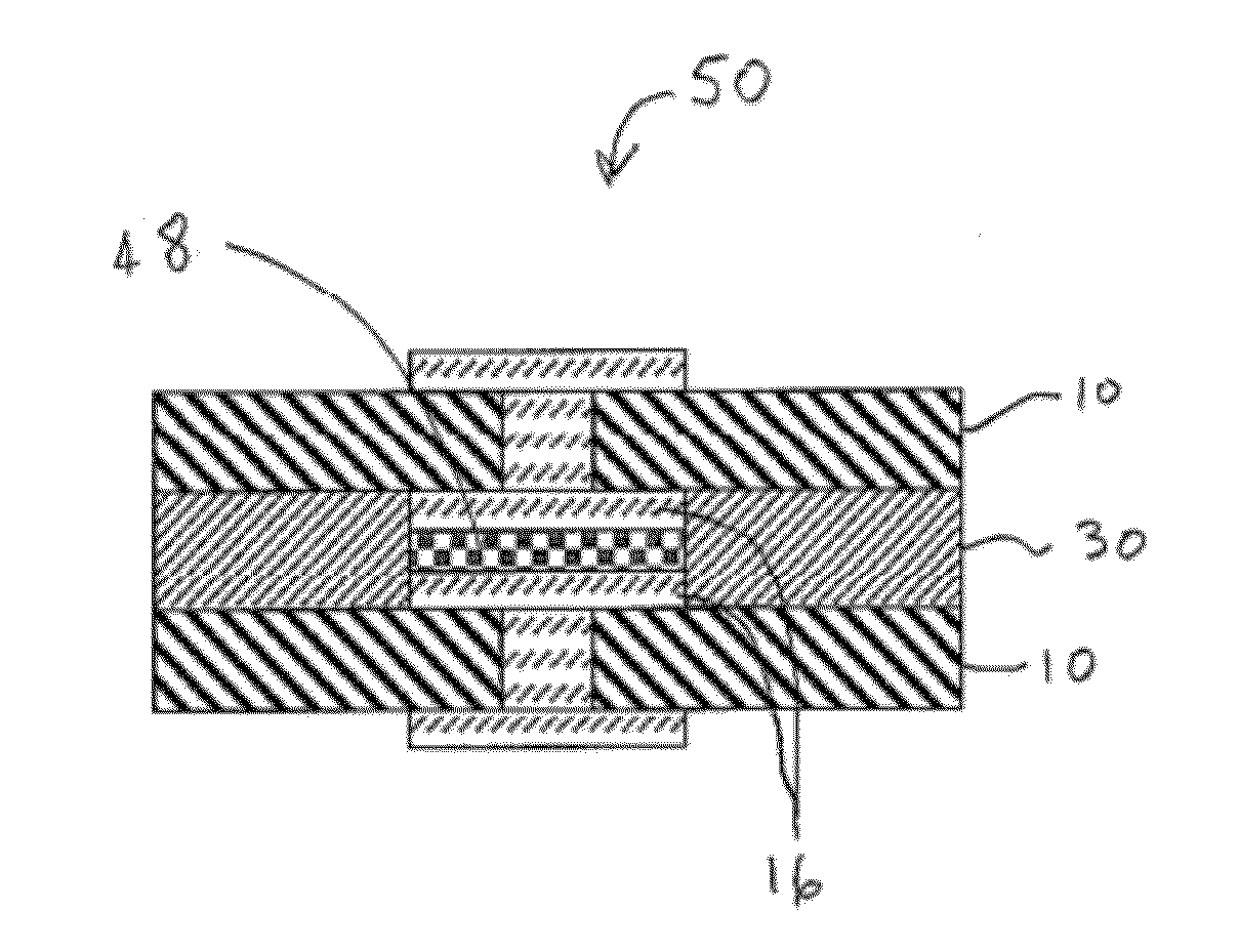
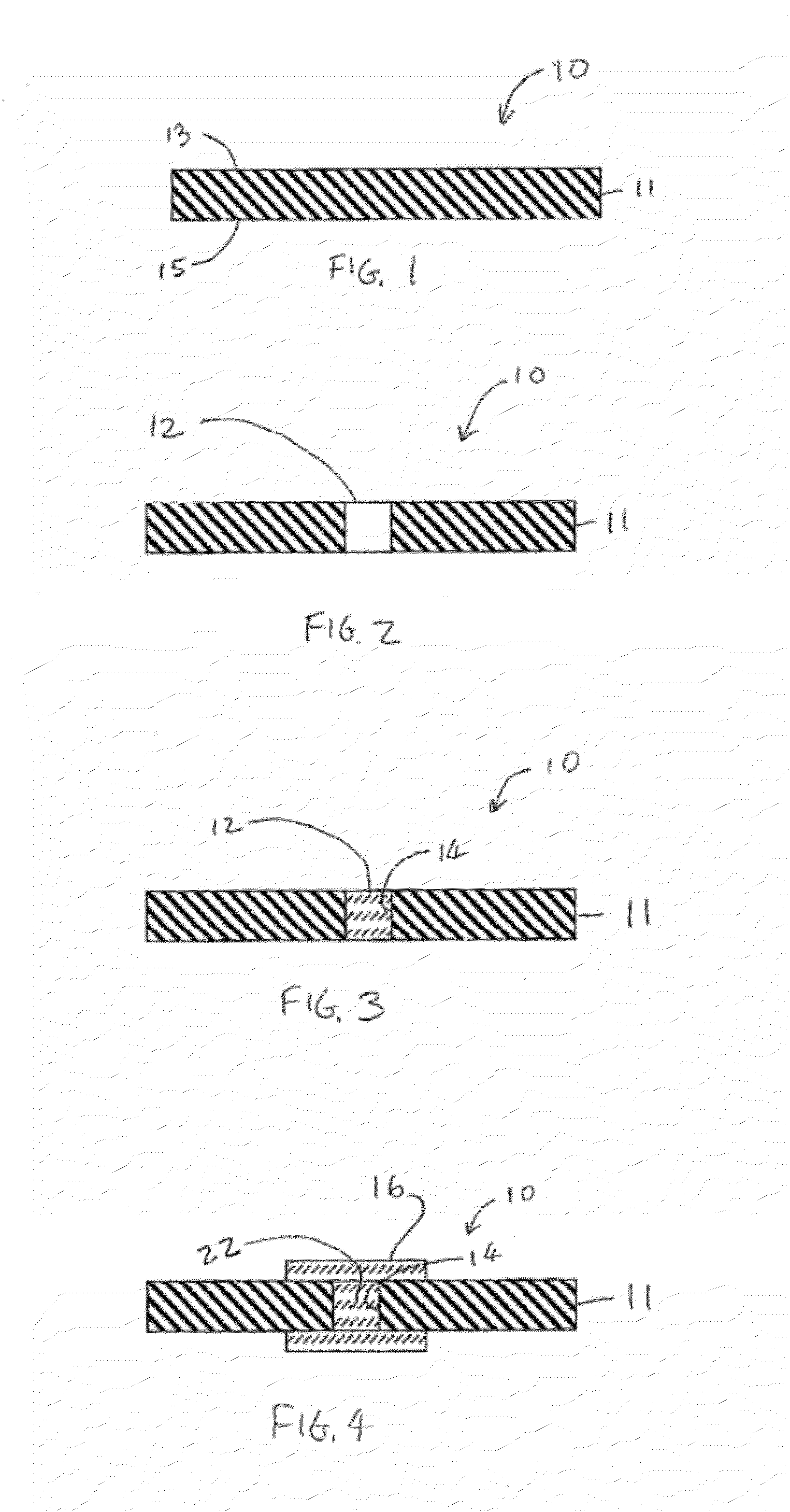
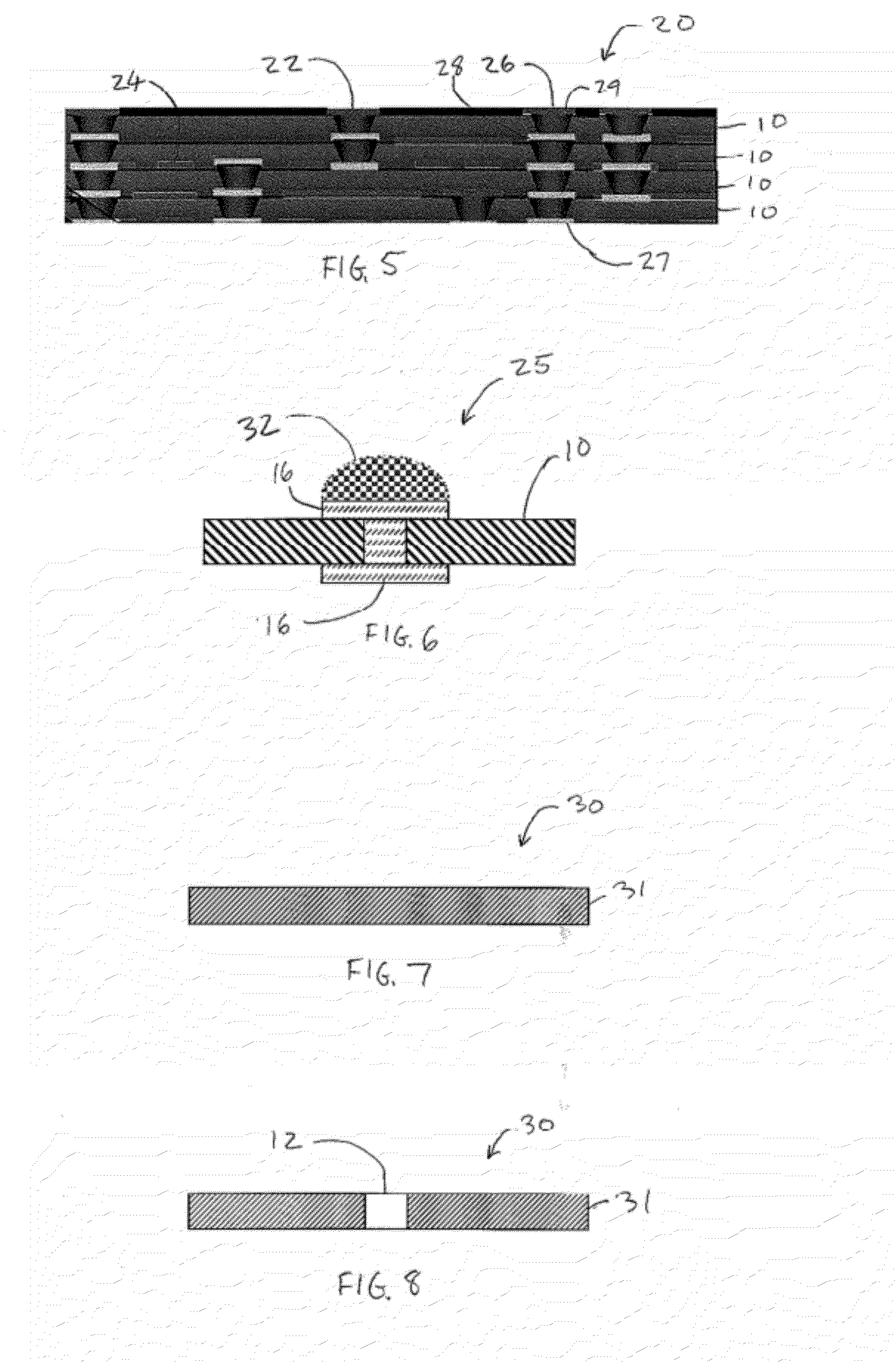
[0052]By the term “circuitized substrate” as used herein is meant a substrate structure having at least one (and preferably more) dielectric layer and at least one external conductive layer positioned on the dielectric layer and including a plurality of conductor pads as part thereof. The dielectric layer(s) may be made of one or more of the following dielectric materials: fiberglass-reinforced epoxy resin (“FR-4”); polytetrafluoroethylene (e.g., Teflon), including polytetrafluoroethylene filled with inorganic particle...


PUM

PropertyMeasurementUnit
thicknessaaaaaaaaaa
volumeaaaaaaaaaa
surface conductiveaaaaaaaaaa

Abstract

A circuitized substrate and method of making same in which quantities of thru-holes are formed within a dielectric interposer layer. The substrate includes two printed circuit board (PCB) layers bonded to opposing sides of the interposer with electrically conductive features of each PCB aligned with the interposer thru-holes. Resistive paste is positioned on the conductive features located adjacent the thru-holes to form controlled electrically resistive connections between conductive features of the two PCBs. A circuitized substrate assembly and method of making same are also disclosed.

Description

FIELD OF THE INVENTION[0001]The present invention relates to circuitized substrates, and more particularly to multilayered circuitized structures such as printed circuit boards (PCBs) and chip carriers, and is particularly related to a PCB structure that utilizes resistor material placed between separated conductive sites prior to lamination, and to a method of making same.BACKGROUND OF THE INVENTION[0002]A common method of forming a multi-layered circuitized substrate involves forming sub-composites each including an individual layer of dielectric material and a layer of electrically conducting material thereon, and then forming electrical circuit patterns in the electrically conductive layer. The conducting material, typically copper, provides signal and voltage planes, as needed. The signal planes are typically in discrete wiring patterns. Voltage planes can be either ground or power planes, and are sometimes collectively referred to as power planes. If required, thru-holes are f...

Claims


Application Information

Patent Timeline
Patent Type & Authority Applications(United States)
IPC IPC(8): H05K1/11H05K3/36
CPCH05K1/162H05K1/167H05K3/4069H05K3/4602H05K3/4614Y10T29/49126H05K3/4623H05K2203/063Y10T29/49165Y10T29/49099H05K3/462
Inventor DAS, RABINDRA N.LAUFFER, JOHN M.MARKOVICH, VOYA R.MCNAMARA, JR., JAMES J.
Owner TTM TECH NORTH AMERICA LLC
Why Eureka
Try Eureka