LED chip

a technology of led chips and led chips, applied in the field of led chips, can solve the problems that the conventional led chips still suffer some problems, and achieve the effect of increasing the light output of the led chip

Inactive Publication Date: 2012-06-21
KING DRAGON INT
View PDF1 Cites 18 Cited by
  • Summary
  • Abstract
  • Description
  • Claims
  • Application Information

AI Technical Summary

Benefits of technology

[0012]One advantage of the present invention is that the heat generated in the PN junction can be conducted outwards quickly through the thermal pad.
[0013]Another advantage of the present invention is that the light emitting area and the light output of the LED chip will be increased.
[0014]Still another advantage of the present invention is that the thermal pad can be isolated from the N type or P type contact pad to achieve ESD protection.

Problems solved by technology

The aforementioned conventional LED chips still suffer some problems.

Method used


Image

  • LED chip
  • LED chip
  • LED chip

Examples


Embodiment Construction

[0024]The invention will now be described with the preferred embodiments and aspects and these descriptions interpret structure and procedures of the invention only for illustrating but not for limiting the Claims of the invention. Therefore, except the preferred embodiments in the specification, the present invention may also be widely used in other embodiments.

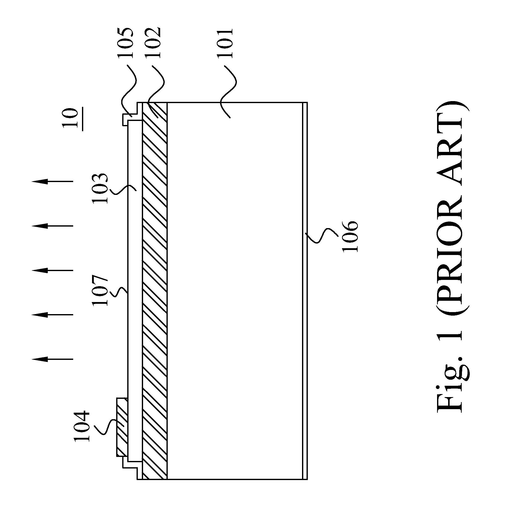
[0025]The present invention discloses a light emitting diode (LED) chip. FIG. 3 illustrates a normal type LED chip. With reference to FIG. 3, in one embodiment of the present invention, the LED chip 30 includes a substrate 301, a first type semiconductor layer, for example, an N type layer 302 disposed on the substrate 301, and a second type semiconductor layer, for example, P type layer 303 disposed on the N type layer 302. The type of the layers may be changeable. The width of the upper layer, in the embodiment the P type layer 303 is substantially longer than that of the lower layer, in the case, the N type layer 302. In ...


PUM


Abstract

The present invention provides a LED chip structure. The LED chip structure comprises a substrate and an N type layer disposed on the substrate; a P type layer disposed on the N type layer; a N type contact pad and a P type contact pad disposed below the substrate; conductive through holes disposed through the substrate to electrically connect the N type layer to the N type contact pad and the P type layer to the conduct heat generated by the P type layer and the N type layer downward.

Description

FIELD OF THE INVENTION[0001]The present invention relates to LED, and more particularly to the structure of a LED chip.BACKGROUND OF THE INVENTION[0002]Light emitting diodes (LEDs) are expected to the source of light for the next generation lighting which will replace incandescent bulbs and fluorescent lights. One conventional LED chip is illustrated in FIG. 1. The convention LED chip 10 includes a substrate 101. A P type layer 102 is formed on the substrate 101, and an N type layer 103 is further formed on the P type layer 102. Then, a passivation layer 105 is formed on two ends of the N type layer 103, and an N type contact pad 104 is formed on the N type layer 103. A terminal contact 106 is formed below the substrate 101. Therefore, the emitting surface 107 is formed on the upper surface of the N type layer 103.[0003]Another conventional LED chip is illustrated in FIG. 2. The convention LED chip 20 includes a substrate 201 (for example made of sapphire). An N type layer 202 is fo...

Claims


Application Information

Patent Timeline
Patent Type & Authority Applications(United States)
IPC IPC(8): H01L33/34H01L33/46
CPCH01L33/382H01L33/641H01L33/44H01L33/405
Inventor YANG, WEN KUN
Owner KING DRAGON INT
Why Eureka
Try Eureka