Oxide material and semiconductor device

Active Publication Date: 2012-06-21
SEMICON ENERGY LAB CO LTD
View PDF5 Cites 19 Cited by
  • Summary
  • Abstract
  • Description
  • Claims
  • Application Information

AI Technical Summary

Benefits of technology

[0008]Another object is to provide a highly reliable semiconductor device which can be manufactured with use of a large-sized substrate such as a mother glass for mass production.
[0011]In view of such problems, an object of one embodiment of the present invention is to provide a semiconductor device including a transistor in which an electron state at an interface between an oxide semiconductor film and a gate insulating film in contact with the oxide semiconductor film is favorable.
[0012]Further, an object of one embodiment of the present invention is to manufacture a highly reliable semiconductor device by giving stable electric characteristics to a transistor in which an oxide semiconductor film is used for a channel.
[0022]According to one embodiment of the present invention, a semiconductor device having excellent electric characteristics can be provided.

Problems solved by technology

When the interface between the oxide semiconductor film and the gate insulating film is in an amorphous state during the manufacturing the transistor or after manufacture of the transistor, the defect density at the interface is high, and thus electric characteristics of the transistor is likely to be unstable.

Method used


Image

  • Oxide material and semiconductor device
  • Oxide material and semiconductor device
  • Oxide material and semiconductor device

Examples


embodiment 1

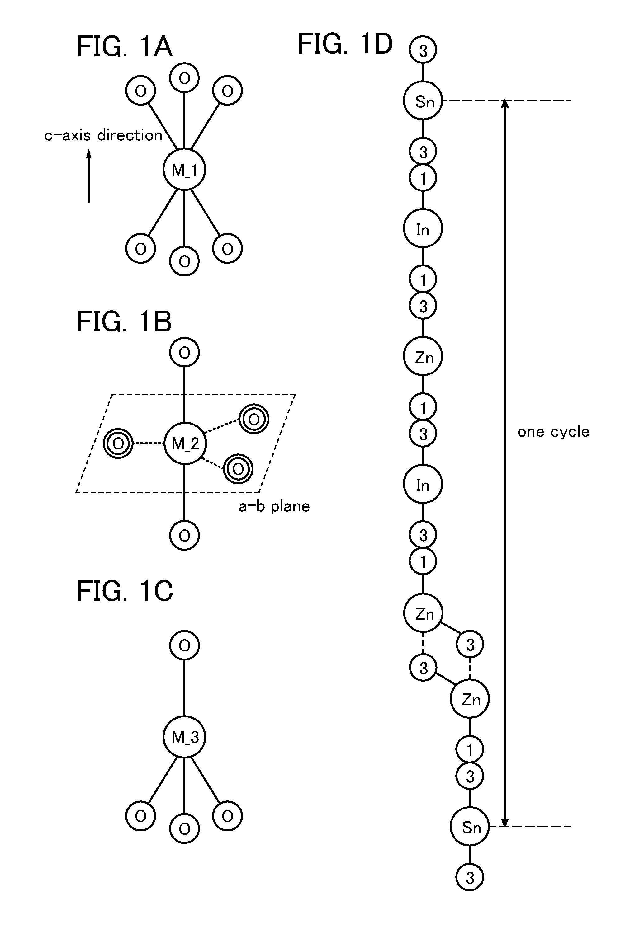
[0054]In this embodiment, a method for forming an oxide film including a crystal with c-axis alignment, which has a triangular or hexagonal atomic arrangement when seen from the direction of an a-b plane, a surface, or an interface, will be described. In the crystal, metal atoms are arranged in a layered manner, or metal atoms and oxygen atoms are arranged in a layered manner along the c-axis, and the direction of the a-axis or the b-axis is varied in the a-b plane (or the surface, or at the interface) (the crystal rotates around the c-axis). Such a crystal is also referred to as a c-axis aligned crystal (CAAC).

[0055]In a broad sense, an oxide including CAAC means a non-single-crystal oxide material including a phase which has a triangular, hexagonal, regular triangular, or regular hexagonal atomic arrangement when seen from the direction perpendicular to the a-b plane and in which metal atoms are arranged in a layered manner or metal atoms and oxygen atoms are arranged in a layered...

embodiment 2

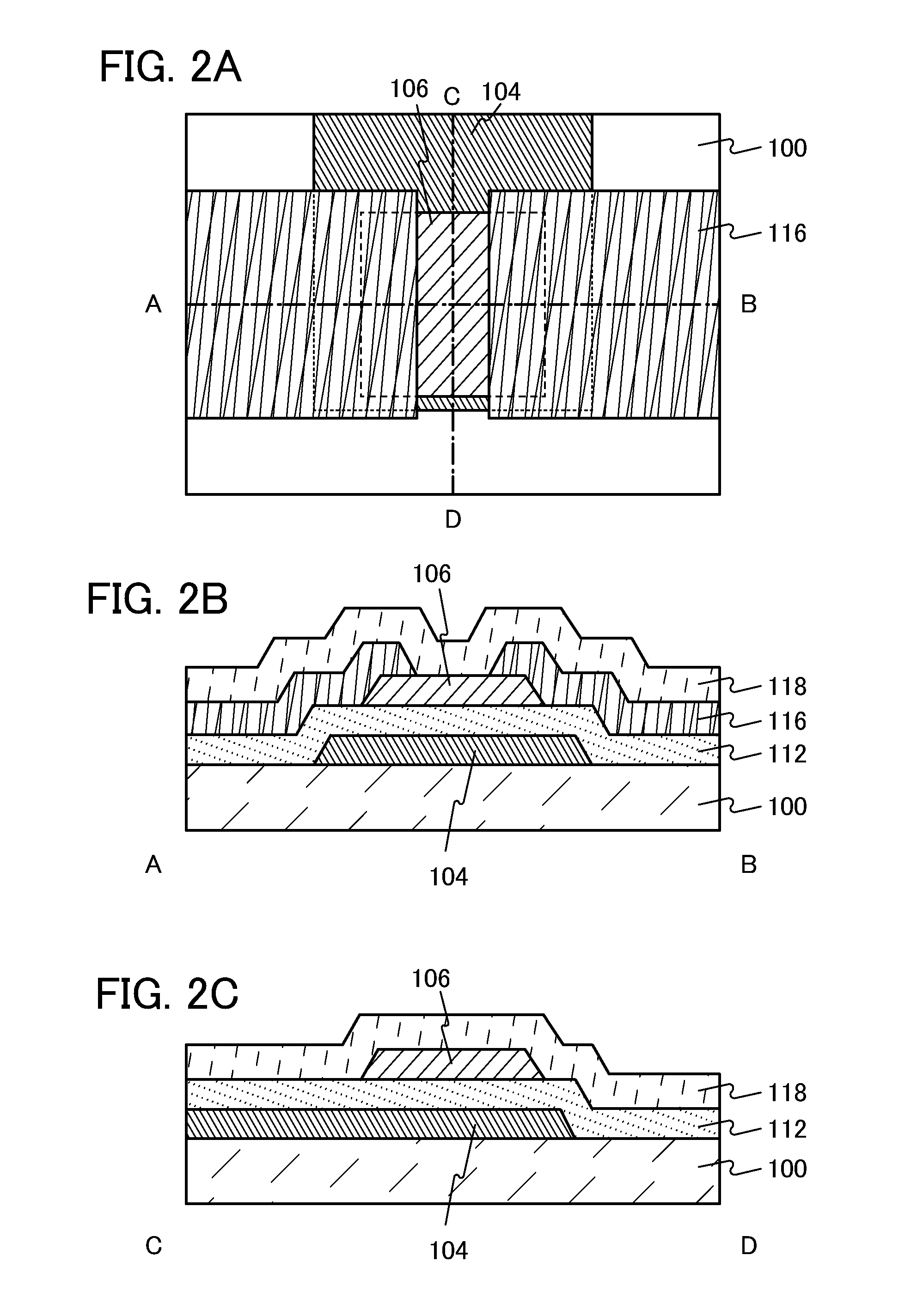
[0082]In this embodiment, an example of a transistor which includes the oxide film including CAAC described in Embodiment 1 will be described with reference to FIGS. 2A to 2C.

[0083]FIG. 2A is a top view of a transistor. FIGS. 2B and 2C illustrate a cross section A-B and a cross section C-D taken along a dashed-dotted line A-B and a dashed-dotted line C-D shown in FIG. 2A.

[0084]The cross section A-B of FIG. 2B is described in detail below.

[0085]The cross section A-B is a cross section of the transistor including a substrate 100, a gate electrode 104 over the substrate 100, a gate insulating film 112 covering the substrate 100 and the gate electrode 104, a semiconductor film 106 over the gate electrode 104 with the gate insulating film 112 positioned therebetween, a pair of electrodes 116 which is over the semiconductor film 106 and partly in contact with the semiconductor film 106, and an interlayer insulating film 118 covering the gate insulating film 112, the semiconductor film 106...

embodiment 3

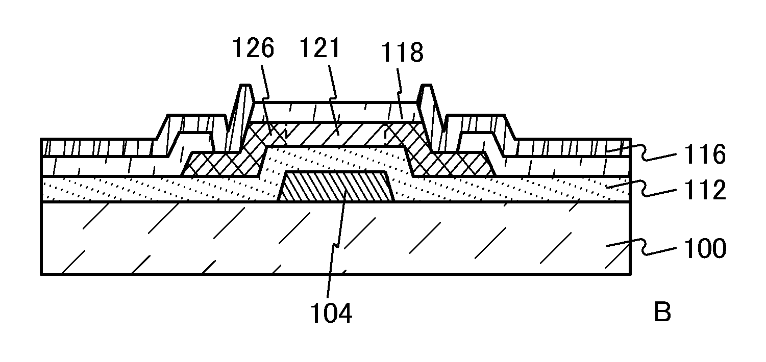
[0110]In this embodiment, a transistor having a structure different from that of the transistor described in Embodiments 2 will be described.

[0111]FIGS. 3A to 3C are a top view and cross-sectional views of a transistor which is one embodiment of the present invention. FIGS. 3B and 3C illustrate a cross section A-B and a cross section C-D taken along a dashed-dotted line A-B and a dashed-dotted line C-D in FIG. 3A.

[0112]The cross section A-B illustrated in FIG. 3B is described in detail below.

[0113]The cross section A-B is a cross-section of the transistor which includes the substrate 100, the gate electrode 104 over the substrate 100, the gate insulating film 112 covering the substrate 100 and the gate electrode 104, the pair of electrodes 116 over the gate insulating film 112, the semiconductor film 106 which is over the gate electrode 104 with the gate insulating film 112 positioned therebetween and partly in contact with the pair of electrodes 116, and the interlayer insulating f...


PUM


Abstract

An object is to provide a material suitably used for a semiconductor included in a transistor, a diode, or the like. Another object is to provide a semiconductor device including a transistor in which the condition of an electron state at an interface between an oxide semiconductor film and a gate insulating film in contact with the oxide semiconductor film is favorable. Further, another object is to manufacture a highly reliable semiconductor device by giving stable electric characteristics to a transistor in which an oxide semiconductor film is used for a channel. A semiconductor device is formed using an oxide material which includes crystal with c-axis alignment, which has a triangular or hexagonal atomic arrangement when seen from the direction of a surface or an interface and rotates around the c-axis.

Description

TECHNICAL FIELD[0001]The present invention relates to a semiconductor device which includes a circuit including a semiconductor element such as a transistor, and a method for manufacturing the semiconductor device. For example, the present invention relates to a power device which is mounted on a power supply circuit; a semiconductor integrated circuit including a memory, a thyristor, a converter, an image sensor, or the like; and an electronic device on which an electro-optical device typified by a liquid crystal display panel, a light-emitting display device including a light-emitting element, or the like is mounted as a component. Moreover, the present invention relates to an oxide used in the semiconductor device.[0002]In this specification, a “semiconductor device” generally refers to a device which can function by utilizing semiconductor characteristics; an electrooptic device, a display device such as a light-emitting display device, a semiconductor circuit, and an electronic...

Claims


Application Information

Patent Timeline
IPC IPC(8): H01L29/78H01B1/00C01B13/00
CPCH01L29/7869C01G19/006H01L29/04H01L29/045H01L29/26H01L29/78696C01P2002/72
Inventor YAMAZAKI, SHUNPEINAKASHIMA, MOTOKIHONDA, TATSUYA
Owner SEMICON ENERGY LAB CO LTD
Why Eureka
Try Eureka