

Thin film transistor, display device having thin film transistor, and method for manufacturing the same
- Summary
- Abstract
- Description
- Claims
- Application Information
AI Technical Summary
Benefits of technology
Problems solved by technology
Method used
Image

Examples
embodiment mode 1
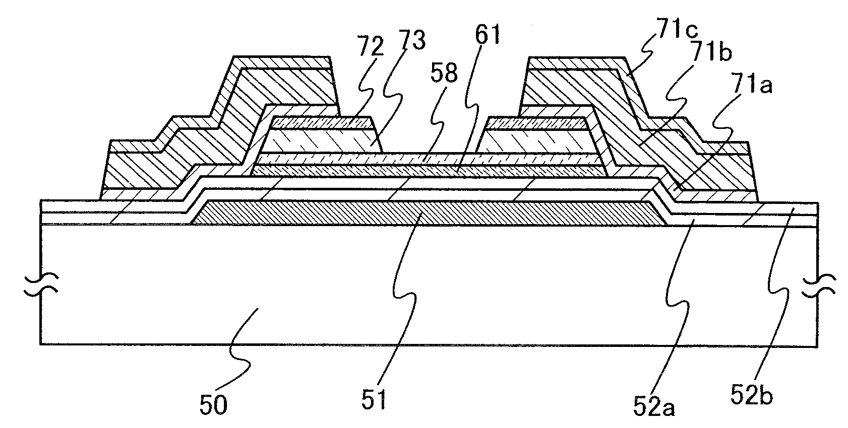
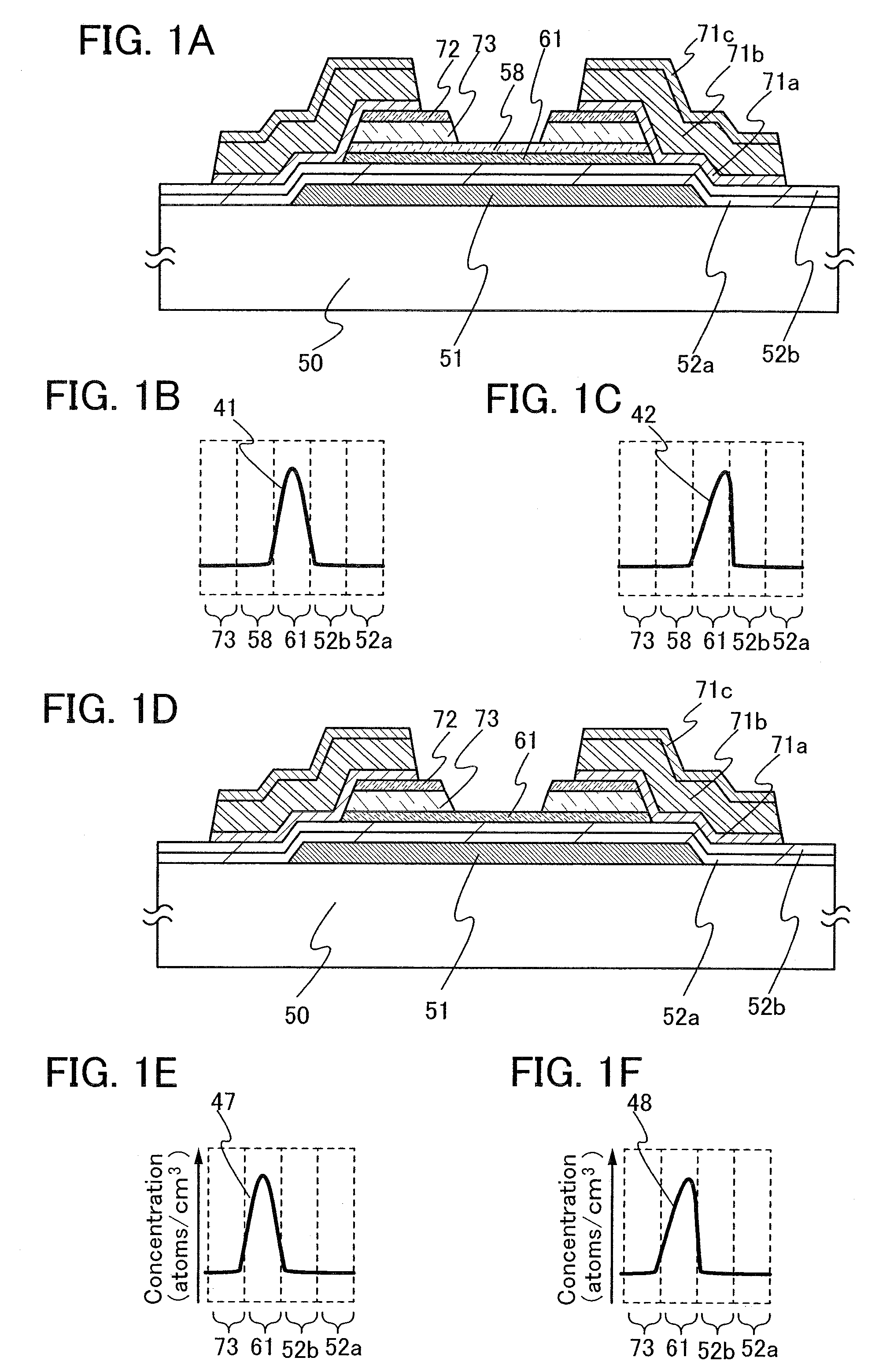
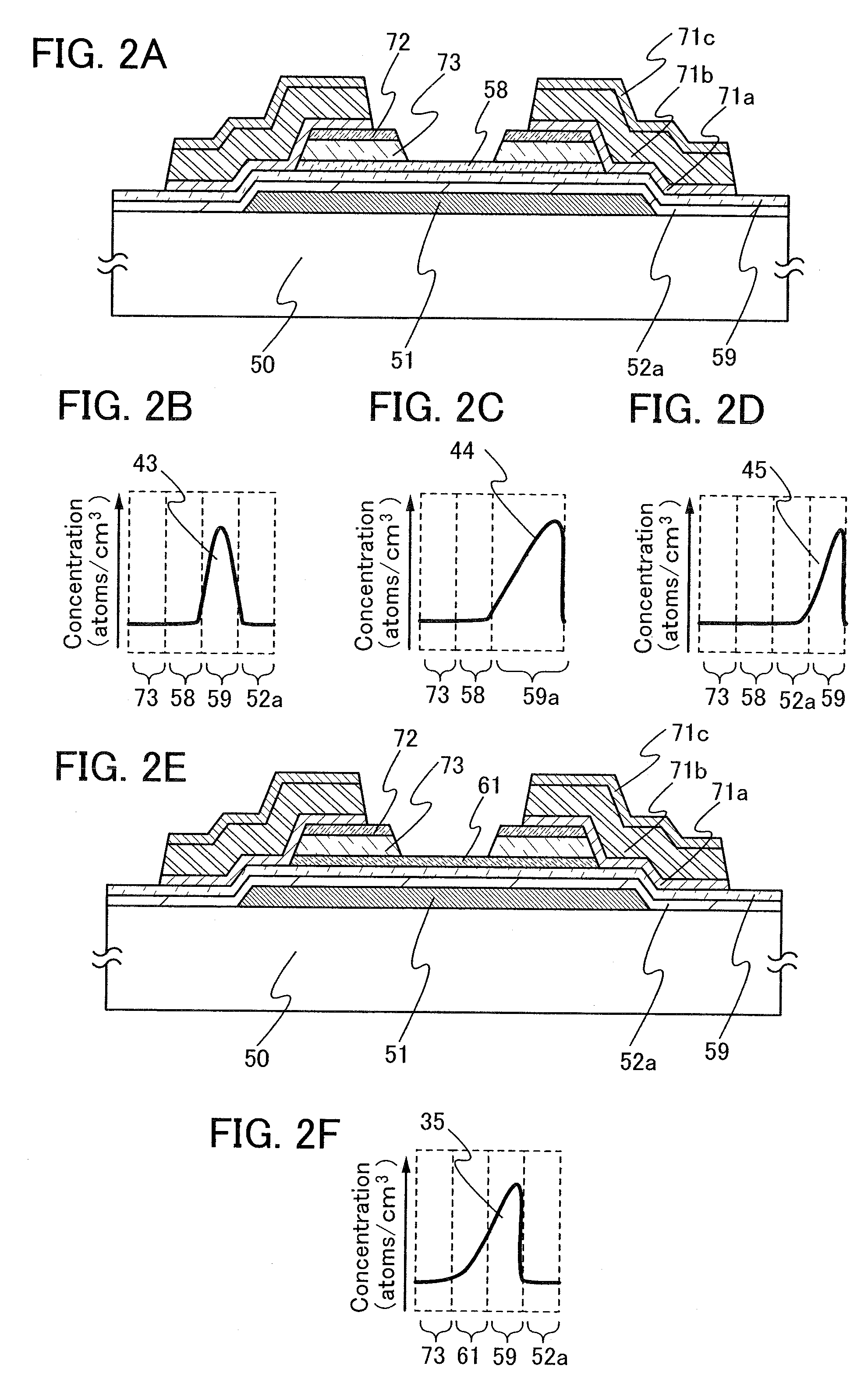
[0092]This embodiment mode describes structures of a thin film transistor which has high crystallinity at an interface between a microcrystalline semiconductor film and a gate insulating film, and has higher field effect mobility and higher on-current than a thin film transistor having a conventional microcrystalline semiconductor film in a channel formation region, with reference to FIGS. 1A to 1F, FIGS. 2A to 2F, FIGS. 3A and 3B, FIGS. 4A to 4D, and FIGS. 5A and 5B.
[0093]In a thin film transistor shown in FIG. 1A, a gate electrode 51 is formed over a substrate 50; gate insulating films 52a and 52b are formed over the gate electrode 51; a microcrystalline semiconductor film 61 including an impurity element which serves as a donor (hereinafter also referred to as the microcrystalline semiconductor film 61) is formed over the gate insulating films 52a and 52b; a microcrystalline semiconductor film 58 not including an impurity element which serves as a donor at a higher concentration ...
embodiment mode 2
[0156]This embodiment mode presents a thin film transistor in which a gate insulating film has a different structure from that of the thin film transistors shown in Embodiment Mode 1, with reference to FIG. 6 and FIGS. 7A to 7D. Here, as shown in FIG. 6 and FIGS. 7A to 7D, the thin film transistor has three gate insulating films instead of the two gate insulating films which are shown in FIGS. 1A to 1F, FIGS. 2A to 2F, FIGS. 3A and 3B, FIGS. 4A to 4D, and FIGS. 5A and 5B.
[0157]Instead of the gate insulating films 52a and 52b of the thin film transistor shown in FIG. 1A, three gate insulating films 52a, 52b, and 52c may be formed as shown in FIG. 6. The gate insulating films 52a and 52b, which are first and second layers, can be formed in a similar manner to Embodiment Mode 1. As the gate insulating film 52c, which is a third layer, a silicon nitride film or a silicon nitride oxide film with a thickness of from 1 to 5 nm approximately can be formed.
[0158]Further, instead of the two g...
embodiment mode 3
[0168]This embodiment mode describes processes for manufacturing the thin film transistors described in Embodiment Mode 1.
[0169]With regard to a thin film transistor including a microcrystalline semiconductor film, an n-channel thin film transistor has higher field effect mobility than a p-channel thin film transistor; thus, an n-channel thin film transistor is more suitable for a driver circuit. Further, it is preferable that all the thin film transistors formed over one substrate have the same polarity so that the number of manufacturing steps is reduced. In description of this embodiment mode, an n-channel thin film transistor is used.
[0170]First, manufacturing processes of the thin film transistors shown in FIGS. 1A and 1D are described below.
[0171]As shown in FIG. 9A, a gate electrode 51 is formed over a substrate 50, and gate insulating films 52a and 52b are formed over the gate electrode 51.
[0172]The gate electrode 51 is formed by a sputtering method, a CVD method, a plating ...
PUM
 Abstract
Description
Claims
Application Information