Semiconductor Device and Manufacturing Method Thereof

Active Publication Date: 2011-08-18
SEMICON ENERGY LAB CO LTD
View PDF96 Cites 12 Cited by
  • Summary
  • Abstract
  • Description
  • Claims
  • Application Information

AI Technical Summary

Benefits of technology

[0010]In view of the above, it is an object of one embodiment of the present invention to provide a semiconductor device having excellent electric characteristics or a manufacturing method thereof. Alternatively, it is an object to provide a semiconductor device having high reliability or a manufacturing method thereof.
[0012]Furthermore, the density of carriers (also referred to as the concentration of carriers) in an oxide semiconductor film has influence on the threshold voltage of the transistor including the oxide semiconductor. The carriers in the oxide semiconductor film are generated due to impurities contained in the oxide semiconductor film. For example, impurities such as a compound containing a hydrogen atom such as H2O, a compound containing a carbon atom, a hydrogen atom, or a carbon atom contained in the deposited oxide semiconductor film increase the density of carriers in an oxide semiconductor film.
[0014]To achieve the above object, in the manufacturing process, plasma damage to at least one of the gate insulating layer, the oxide semiconductor layer, and the interface therebetween is suppressed. Further, impurities that influence on the density of carriers in the oxide semiconductor film, for example, a compound containing a hydrogen atom such as H2O or a hydrogen atom, may be removed.
[0027]According to one embodiment of the disclosed invention, one or both of the following effects can be obtained.
[0029]According to one embodiment of the present invention, a semiconductor device having high reliability or a manufacturing method thereof can be provided.

Problems solved by technology

However, a semiconductor element including an oxide semiconductor has not had excellent characteristics yet.
In a manufacturing process of a transistor, when plasma damage is caused at the interface between a gate insulating layer and an oxide semiconductor layer, a defect (an interface trap) is caused at the interface between the gate insulating layer and the oxide semiconductor layer.
Further, when the plasma damage is caused in one or both of the gate insulating layer and the oxide semiconductor layer, a defect (an in-film trap) is caused.
These defects cause a threshold voltage shift of the transistor.

Method used


Image

  • Semiconductor Device and Manufacturing Method Thereof
  • Semiconductor Device and Manufacturing Method Thereof
  • Semiconductor Device and Manufacturing Method Thereof

Examples


embodiment 1

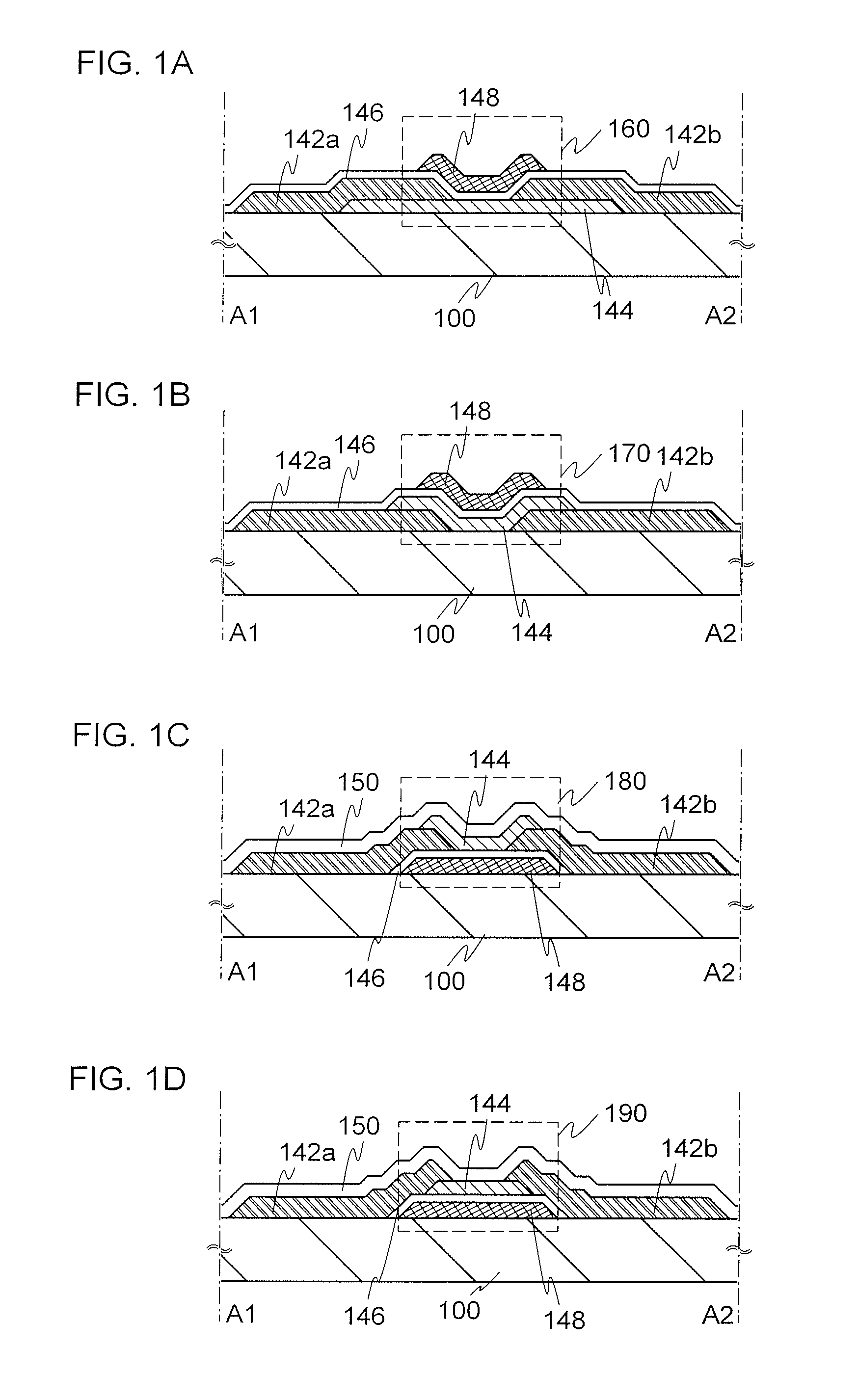
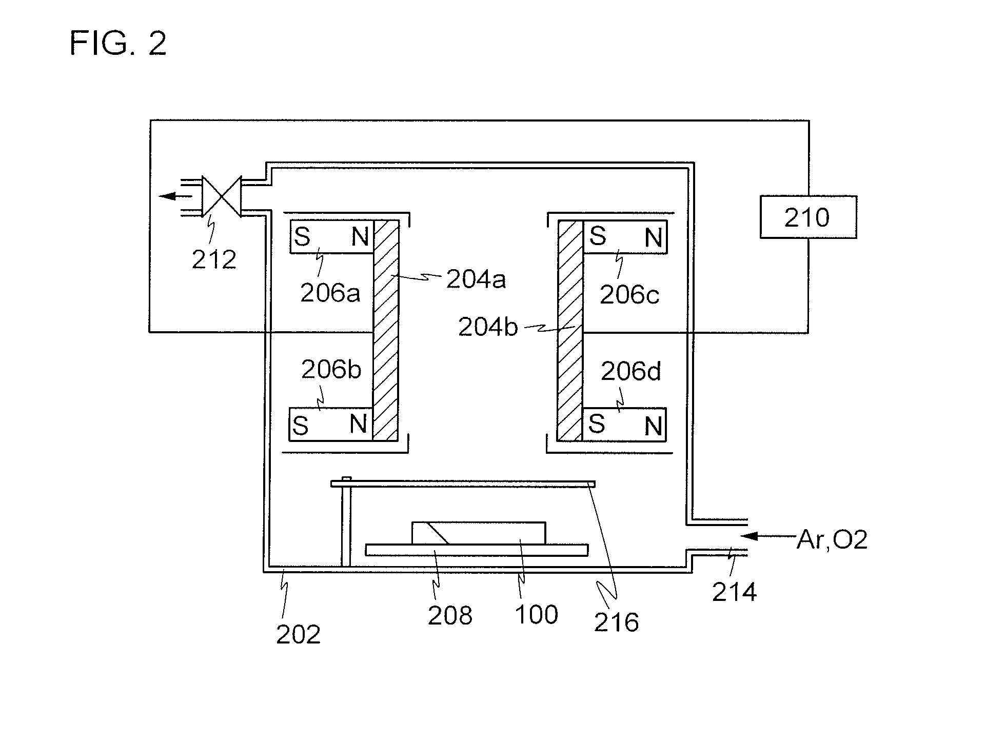
[0043]In this embodiment, an example of a structure of a semiconductor device and a manufacturing process thereof according to one embodiment of the disclosed invention will be described with reference to FIGS. 1A to 1D, FIG. 2, FIGS. 3A to 3B, and FIGS. 4A to 4C.

[0044]In FIGS. 1A to 1D, cross-sectional structures of transistors are illustrated as examples of semiconductor devices.

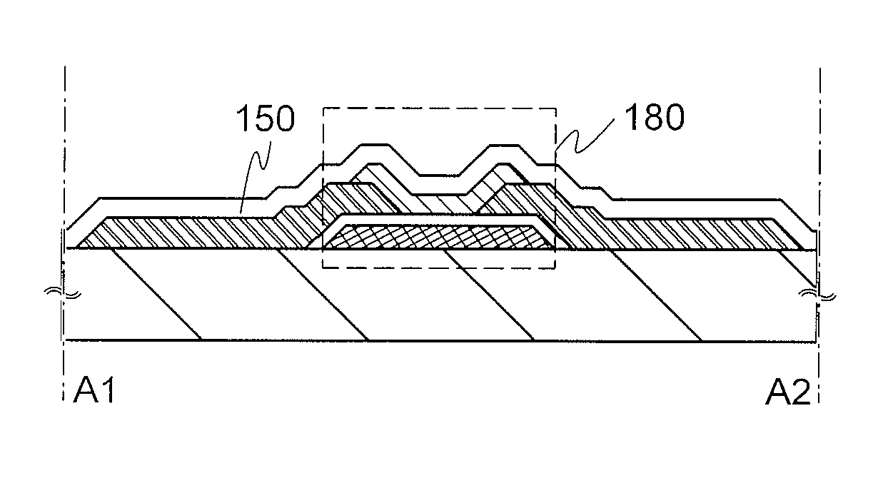
[0045]A transistor 160 illustrated in FIG. 1A is an example of a top-gate transistor. The transistor 160 includes, over a substrate 100, an oxide semiconductor layer 144, a source electrode 142a and a drain electrode 142b in contact with the oxide semiconductor layer 144, a gate insulating layer 146 covering at least a channel formation region of the oxide semiconductor layer 144, the source electrode 142a, and the drain electrode 142b, and a gate electrode 148 provided over the gate insulating layer 146 and overlapping with the channel formation region of the oxide semiconductor layer 144.

[0046]A transist...

embodiment 2

[0120]In this embodiment, an external view and a cross section of a liquid crystal display panel, which is an embodiment of a semiconductor device of the present invention, will be described with reference to FIGS. 6A to 6C. The liquid crystal display panel illustrated in FIGS. 6A to 6C includes transistors illustrated in Embodiment 1. FIGS. 6A and 6C are plan views of panels in each of which thin film transistors 4010 and 4011 and a liquid crystal element 4013 are sealed between a first substrate 4001 and a second substrate 4006 with a sealant 4005. FIG. 6B is a cross-sectional view taken along line M-N in FIG. 6A or FIG. 6C.

[0121]The sealant 4005 is provided to surround a pixel portion 4002 and a scan line driver circuit 4004 which are provided over the first substrate 4001. The second substrate 4006 is provided over the pixel portion 4002 and the scan line driver circuit 4004. Therefore, the pixel portion 4002 and the scan line driver circuit 4004 are sealed together with a liqui...

embodiment 3

[0142]In this embodiment, an example of an electronic paper will be described as an embodiment of a semiconductor device.

[0143]The thin film transistor described in Embodiment 1 can be used for electronic paper in which electronic ink is driven by an element electrically connected to a switching element. The electronic paper is also referred to as an electrophoretic display device (an electrophoretic display) and is advantageous in that it has the same level of readability as plain paper, it has lower power consumption than other display devices, and it can be made thin and lightweight.

[0144]There are a variety of modes of electrophoretic displays. Electrophoretic displays contain a plurality of microcapsules dispersed in a solvent or a solute, each microcapsule containing first particles that are positively charged and second particles that are negatively charged. By applying an electric field to the microcapsules, the particles in the microcapsules move in opposite directions to e...


PUM


Abstract

It is an object to provide a semiconductor device having excellent electric characteristics or high reliability, or a manufacturing method thereof. A semiconductor device including a gate electrode, an oxide semiconductor layer overlapping with the gate electrode, a source electrode and a drain electrode in contact with the oxide semiconductor layer, and a gate insulating layer provided between the gate electrode and the oxide semiconductor layer is provided. The oxide semiconductor layer is formed by a facing target sputtering method. The carrier concentration of the oxide semiconductor is less than 1×10¹² / cm3.

Description

BACKGROUND OF THE INVENTION[0001]1. Field of the Invention[0002]The technical field of the present invention relates to a semiconductor device and a manufacturing method of the semiconductor device. Here, semiconductor devices refer to general elements and devices that function by utilizing semiconductor characteristics.[0003]2. Description of the Related Art[0004]A technique in which a semiconductor device such as a transistor is manufactured using an oxide semiconductor as a semiconductor material and the semiconductor device is applied to a semiconductor integrated circuit and an electronic device has attracted attention. For example, Patent Document 1 and Patent Document 2 disclose a technique in which a transistor is manufactured using zinc oxide or an In—Ga—Zn—O-based oxide semiconductor as a semiconductor material and such a transistor is used as a switching element or the like of an image display device.[0005]A transistor in which a channel formation region (also referred to...

Claims


Application Information

Patent Timeline
IPC IPC(8): H01L29/786H01L21/34
CPCH01L21/02554H01L21/02565H01L29/66969H01L29/7869H01L21/02631
Inventor YAMAZAKI, SHUNPEI
Owner SEMICON ENERGY LAB CO LTD
Why Eureka
Try Eureka