Transistor, Semiconductor Device Comprising the Transistor and Method for Manufacturing the Same

a semiconductor device and transistor technology, applied in the direction of semiconductor devices, radio frequency controlled devices, electrical apparatus, etc., can solve the problems of requiring additional polysilicon filling, damage to already formed structures, and formation of back gate contacts, so as to reduce manufacturing costs and simplify manufacturing processes

Active Publication Date: 2012-06-21
INST OF MICROELECTRONICS CHINESE ACAD OF SCI
View PDF3 Cites 206 Cited by
  • Summary
  • Abstract
  • Description
  • Claims
  • Application Information

AI Technical Summary

Benefits of technology

[0010]In an embodiment, the semiconductor device may comprise at least one N-type field effect transistor (NFET) and at least one P-type field effect transistor (PFET). The at least one N-type field effect transistor and the at least one P-type field effect transistor may be isolated from each other by isolators. The isolator may be a shallow trench isolation, for example.
[0011]According to yet another aspect, a method for manufacturing a transistor is provided. The method forms an epitaxial part raised from the surface of a back gate electrode using an epitaxy process and thus forms a back gate contact. As compared to a conventional method, the formation of a back gate contact in such a manufacturing method will not damage the structures already formed and there is no need for an additional protective layer and additional polysilicon filling, thereby greatly simplifying the manufacturing process and significantly reducing the cost of manufacture.

Problems solved by technology

However, in the existing manufacturing flow for the semiconductor device or integrated circuits, the formation of the back gate contact may damage the structures already formed.
For example, in the process flow of forming a device by the SOI technology, the formation of the back gate contact will probably damage a buried insulating layer or a buried oxide (BOX) layer in an SOI substrate.
Furthermore, the formation of the back gate contact requires an additional polysilicon filling.
This makes the manufacturing process become particularly complex, and meanwhile increases the cost of manufacture.

Method used


Image

  • Transistor, Semiconductor Device Comprising the Transistor and Method for Manufacturing the Same
  • Transistor, Semiconductor Device Comprising the Transistor and Method for Manufacturing the Same
  • Transistor, Semiconductor Device Comprising the Transistor and Method for Manufacturing the Same

Examples


Embodiment Construction

[0031]The exemplary embodiments of the invention will be described in detail with reference to the accompanying drawings hereinafter. The drawings are schematic and not drawn to scale, and just for illustrating the embodiments of the invention and are not intended to limit the protective scope of the invention. In the drawings, like reference numerals denote identical or similar components. For making the technical solution of the invention clearer, process steps and structures of a device well known in the art are omitted herein.

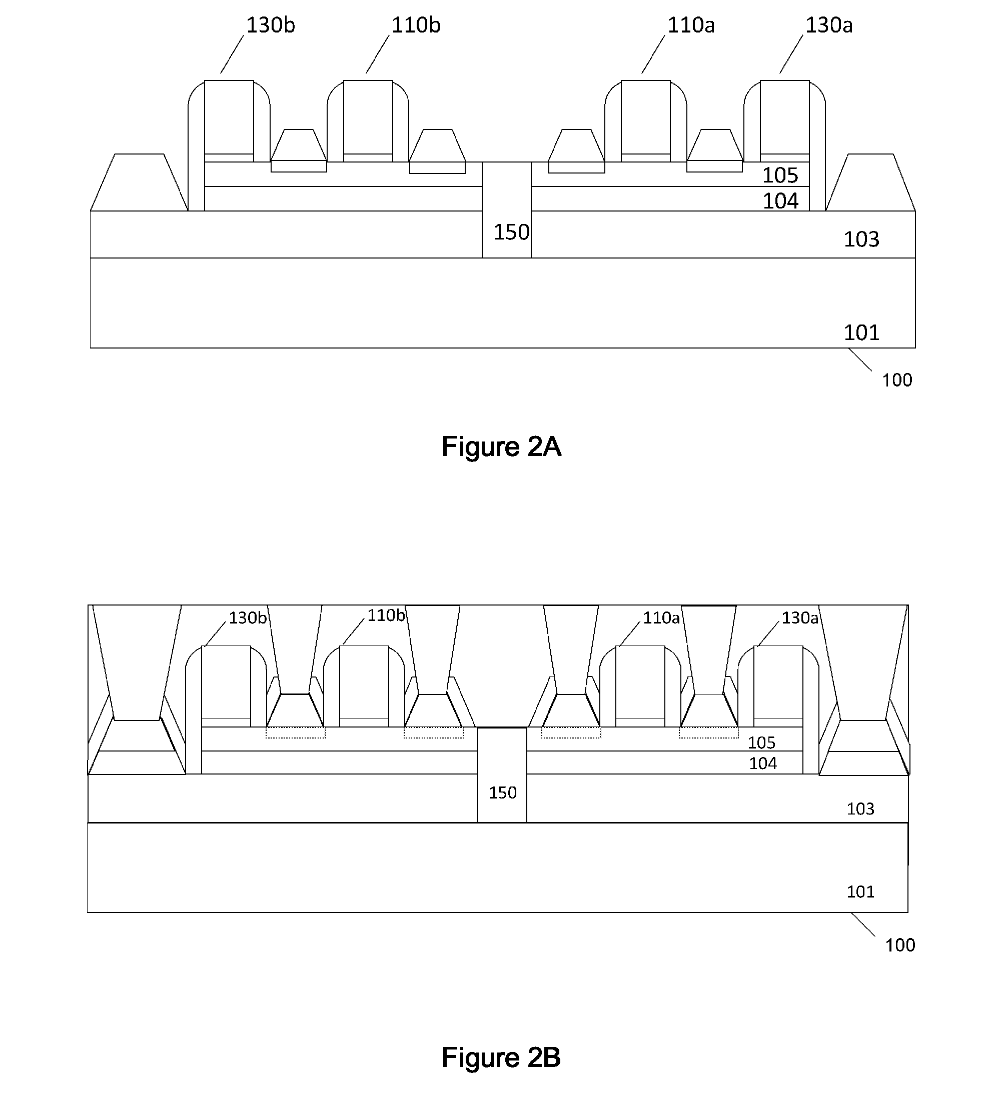
[0032]First, a transistor according to an exemplary embodiment of the invention is described in detail with reference to FIGS. 1A and 1B.

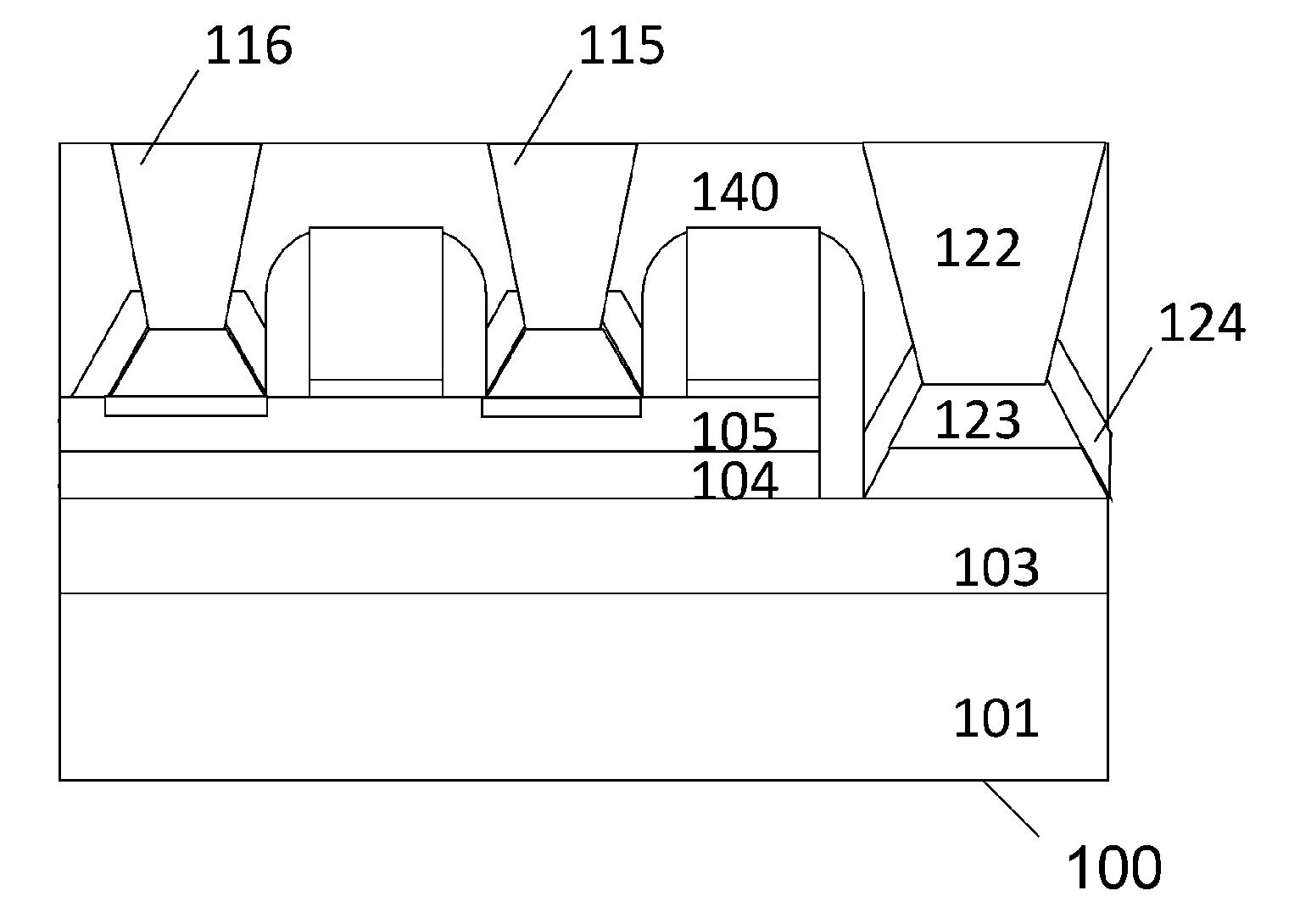
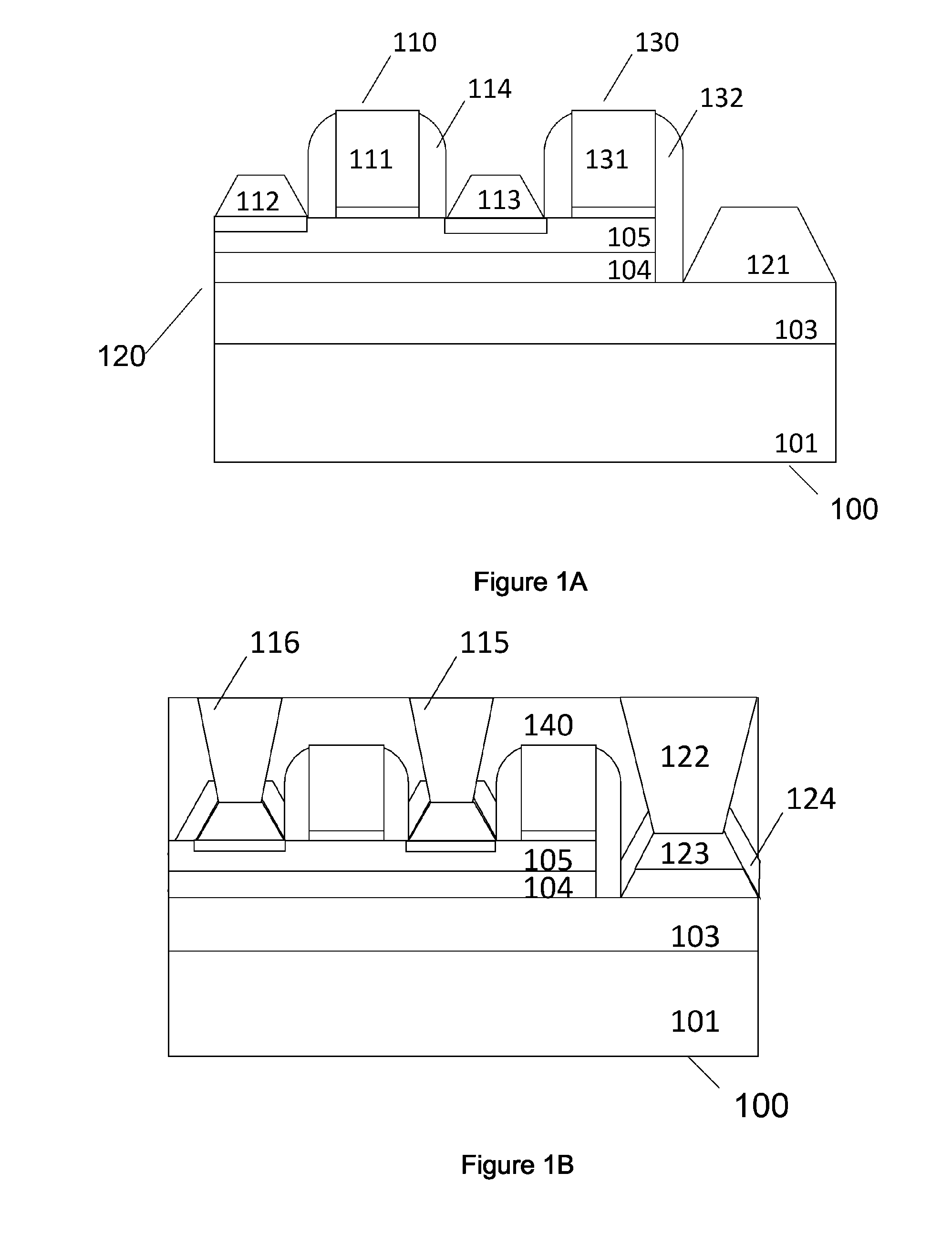
[0033]FIG. 1A shows a schematic cross section view of a transistor according to an exemplary embodiment of the invention.

[0034]As shown in FIG. 1A, a substrate 100 for forming a transistor 110 may comprise a base layer 101, a first semiconductor layer 103, an insulating layer 104 and a second semiconductor layer 105 stacke...


PUM


Abstract

The invention relates to a transistor, a semiconductor device comprising the transistor and manufacturing methods for the transistor and the semiconductor device. The transistor according to the invention comprises: a substrate comprising at least a base layer, a first semiconductor layer, an insulating layer and a second semiconductor layer stacked sequentially; a gate stack formed on the second semiconductor layer; a source region and a drain region located on both sides of the gate stack respectively; a back gate comprising a back gate dielectric and a back gate electrode formed by the insulating layer and the first semiconductor layer, respectively; and a back gate contact formed on a portion of the back gate electrode. The back gate contact comprises an epitaxial part raised from the surface of the back gate electrode, and each of the source region and the drain region comprises an epitaxial part raised from the surface of the second semiconductor layer. As compared to a conventional transistor, the manufacturing process of the transistor of the invention is simplified and the cost of manufacture is reduced.

Description

FIELD OF THE INVENTION[0001]The invention relates to a transistor and a semiconductor device comprising the transistor. More specifically, the invention relates to a transistor comprising a back gate and a semiconductor device comprising the transistor. The invention also relates to methods for manufacturing the transistor and the semiconductor device.BACKGROUND OF THE INVENTION[0002]Transistors are commonly used elements in integrated circuits. In a CMOS circuit formed by CMOS technology, an N-channel transistor and a P-channel transistor are usually included.[0003]With the development of the semiconductor technology, a transistor comprising a back gate appears. Compared with a transistor comprising only a front gate or a gate stack, the transistor including a back gate has improved performance. A back gate contact realizing a desired electrical connection between the back gate and the other components in the circuit is one of the key components in the circuit.[0004]In current semi...

Claims


Application Information

Patent Timeline
Patent Type & Authority Applications(United States)
IPC IPC(8): H01L29/772H01L21/8238H01L21/336
CPCH01L21/8213H01L21/8252H01L21/84H01L29/78648H01L27/1203H01L29/66545H01L29/66628H01L27/0605
Inventor LIANG, QINGQINGZHU, HUILONGZHONG, HUICAI
Owner INST OF MICROELECTRONICS CHINESE ACAD OF SCI
Why Eureka
Try Eureka