Semiconductor circuit and semiconductor device

a semiconductor and circuit technology, applied in semiconductor devices, electronic switching, pulse techniques, etc., can solve the problems of delay in transmission, no dv/dt generation, and turning off the p-side semiconductor switching devi

Active Publication Date: 2012-06-21
MITSUBISHI ELECTRIC CORP
View PDF2 Cites 8 Cited by
  • Summary
  • Abstract
  • Description
  • Claims
  • Application Information

AI Technical Summary

Benefits of technology

[0011]It is an object of the present invention to provide a semiconductor circuit and a semiconductor device both of which have a general-purpose malfunction prevention function by which a malfunction due to dV / dt can be prevented without being affected by any external factor.

Problems solved by technology

In this case, dV / dt is an abrupt change in a reference potential generated by ON / OFF operations of a semiconductor switching device described later and can cause a malfunction.
There is a case, however, where no dV / dt is generated until the ON-side one-shot signal is finished because of light load driving of the semiconductor circuit, a delay in response of the P-side semiconductor switching device, a delay in transmission of the level shift circuit, and the like.
At that time, since a circuit structure for decreasing a resistance value of the other system is invalidated and the resistance value of the OFF side is higher than that of the ON side, when dV / dt is applied, an OFF-side pulse is transmitted earlier to a Set-Reset Flip-Flop and this disadvantageously turns off the P-side semiconductor switching device.
Increasing the width of the one-shot signal, however, arises a problem that a time period while the high voltage transistor is in an ON state becomes longer and the power consumed in the high voltage transistor is increased.

Method used


Image

  • Semiconductor circuit and semiconductor device
  • Semiconductor circuit and semiconductor device
  • Semiconductor circuit and semiconductor device

Examples


Embodiment Construction

A. The First Preferred Embodiment

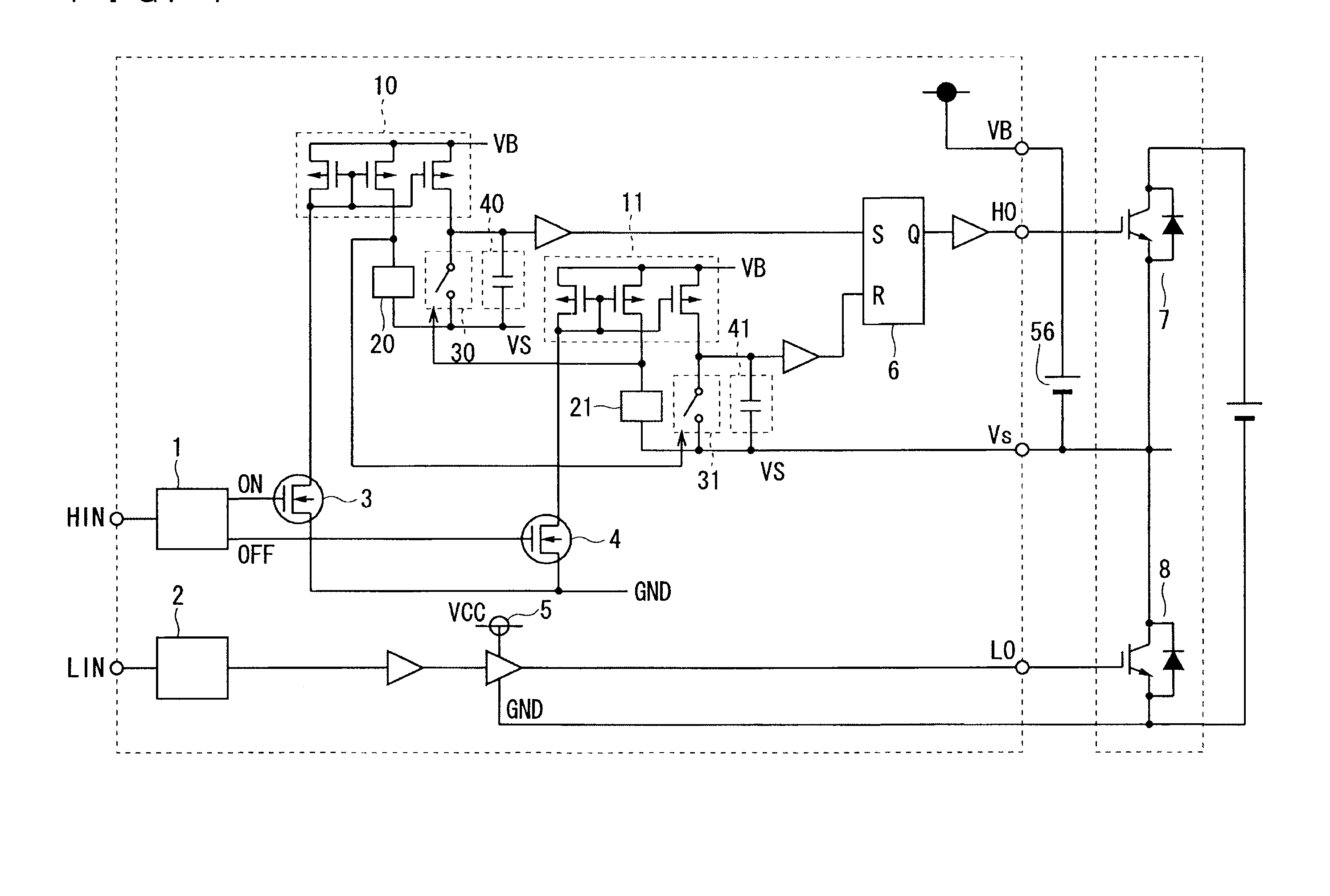
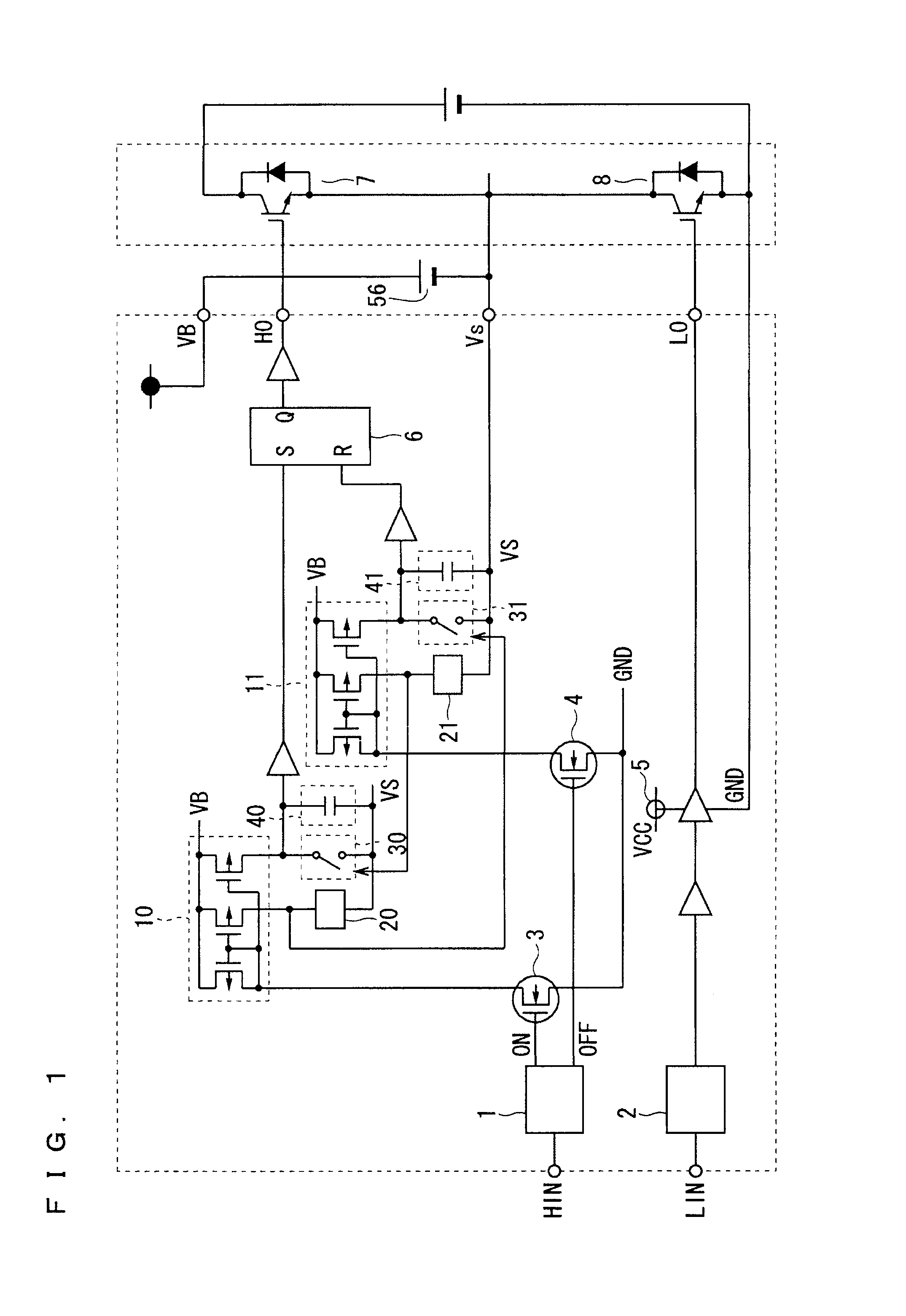
[0022]FIG. 10 is a circuit diagram showing a semiconductor circuit (level shift circuit) in accordance with an underlying technique of the present invention, which is disclosed in Japanese Patent Application Laid Open Gazette No. 9-172366.

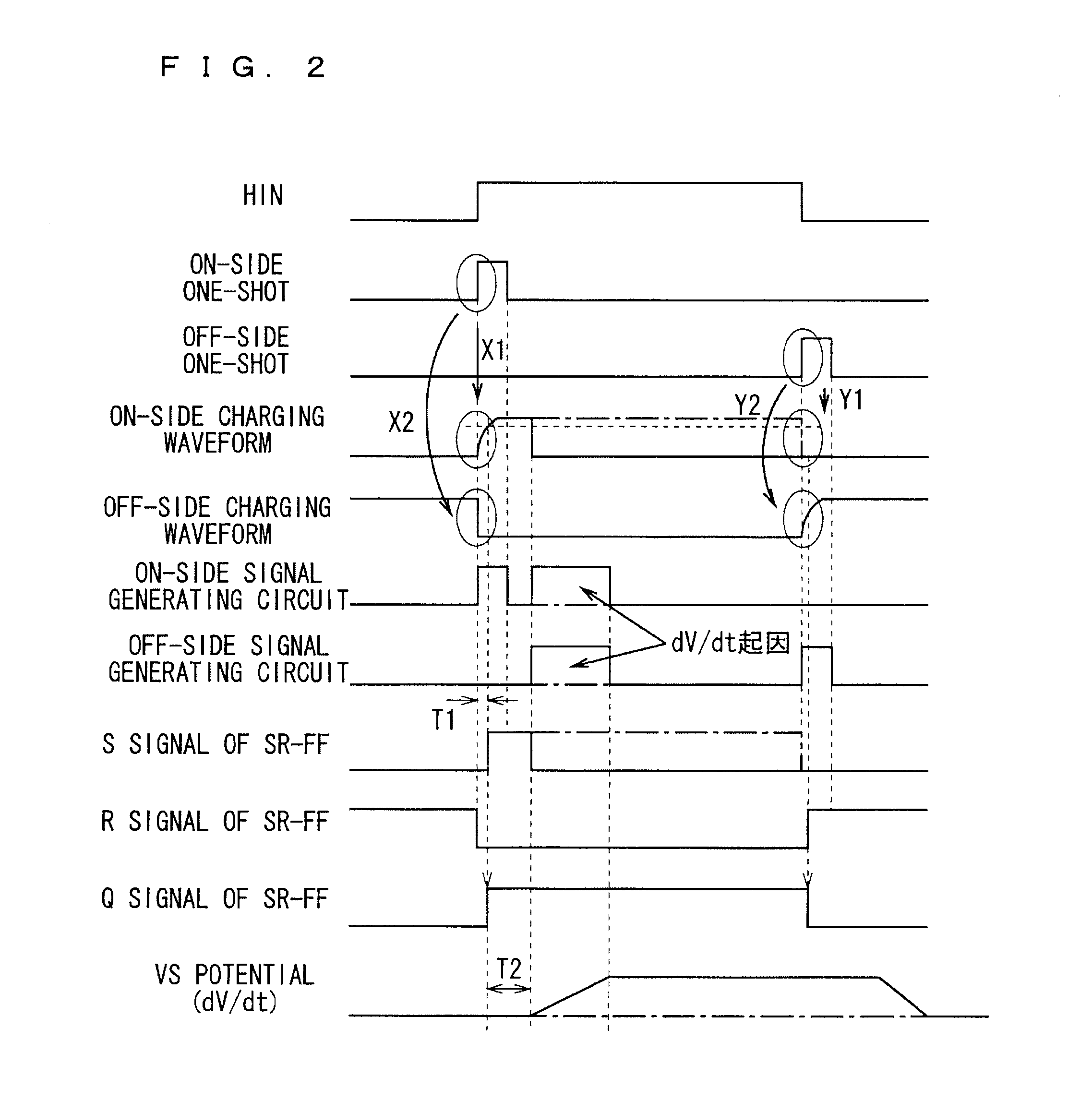
[0023]This level shift circuit uses respective one-shot signals both on ON / OFF sides to drive a high voltage transistors 109a and 109b and further uses a drain current and a resistance value which are thereby generated, to generate a voltage signal.

[0024]Between a system for transmitting an ON-side signal and a system for transmitting an OFF-side signal, interposed is a circuit structure for decreasing a resistance value in the other system at the instant when each signal is transmitted, and the circuit structure is set so that the voltage drop in resistors Ra and Rb due to the dV / dt can become larger in the system for transmitting the OFF-side signal.

[0025]When the generated voltage signal reaches a threshold value...


PUM


Abstract

A semiconductor circuit of the present invention comprises a capacitor for charging ON driven electric charges in response to an ON driving signal, a capacitor for charging OFF driven electric charges in response to an OFF driving signal, a signal generating circuit for generating a first trigger signal in response to the ON driving signal, a signal generating circuit for generating a second trigger signal in response to the OFF driving signal, a discharging circuit for discharging the ON driven electric charges in response to the second trigger signal, and a discharging circuit for discharging the OFF driven electric charges in response to the first trigger signal. With this configuration, it is possible to provide a semiconductor circuit and a semiconductor device both of which have a general-purpose malfunction prevention function by which a malfunction due to dV/dt can be prevented without being affected by any external factor.

Description

BACKGROUND OF THE INVENTION[0001]1. Field of the Invention[0002]The present invention relates to a semiconductor circuit and a semiconductor device, and more particularly to a semiconductor circuit and a semiconductor device both for driving a power semiconductor switching element.[0003]2. Description of the Background Art[0004]Some of level shift circuits included in semiconductor circuits which drive conventional power semiconductor switching elements perform, for example, a function for preventing a malfunction due to self-excited dV / dt (an abrupt change in a floating potential VM generated when a P-side semiconductor switching device is turned off) and another function for preventing a malfunction due to separately excited dV / dt (an abrupt change in a floating potential VM generated by ON / OFF operations of other arms) (see Paragraph [0014] and “Means for Solving the Problems” of Japanese Patent Application Laid Open Gazette No. 9-172366). In this case, dV / dt is an abrupt change ...

Claims


Application Information

Patent Timeline
Patent Type & Authority Applications(United States)
IPC IPC(8): H03K3/356
CPCH03K17/162H01L2924/0002H01L2924/00
Inventor IMANISHI, MOTOKISAKAI, KENJITANAKA, YOSHIKAZUOYAMA, KYOUKO
Owner MITSUBISHI ELECTRIC CORP
Why Eureka
Try Eureka